Verilog interview Questions
How to write FSM is verilog?
there r mainly 4 ways 2 write fsm code
1) using 1 process where all input decoder, present state, and output decoder r combine in one process.
2) using 2 process where all comb ckt and sequential ckt separated in different process
3) using 2 process where input decoder and persent state r combine and output decoder seperated in other process
4) using 3 process where all three, input decoder, present state and output decoder r separated in 3 process.
(Also refer to Tutorial section for more)
Verilog interview Questions
21)What is difference between freeze deposit and force?
$deposit(variable, value);
This system task sets a Verilog register or net to the specified value. variable is the
register or net to be changed; value is the new value for the register or net. The value
remains until there is a subsequent driver transaction or another $deposit task for the
same register or net. This system task operates identically to the ModelSim
force -deposit command.
The force command has -freeze, -drive, and -deposit options. When none of these is
specified, then -freeze is assumed for unresolved signals and -drive is assumed for resolved
signals. This is designed to provide compatibility with force files. But if you prefer -freeze
as the default for both resolved and unresolved signals.
Verilog interview Questions
22)Will case infer priority register if yes how give an example?
yes case can infer priority register depending on coding style
reg r;
// Priority encoded mux,
always @ (a or b or c or select2)
begin
r = c;
case (select2)
2'b00: r = a;
2'b01: r = b;
endcase
end
Verilog interview Questions
23)Casex,z difference,which is preferable,why?
CASEZ :
Special version of the case statement which uses a Z logic value to represent don't-care bits. CASEX :
Special version of the case statement which uses Z or X logic values to represent don't-care bits.
CASEZ should be used for case statements with wildcard don’t cares, otherwise use of CASE is required; CASEX should never be used.
This is because:
Don’t cares are not allowed in the "case" statement. Therefore casex or casez are required. Casex will automatically match any x or z with anything in the case statement. Casez will only match z’s -- x’s require an absolute match.
Verilog interview Questions
24)Given the following Verilog code, what value of "a" is displayed?
always @(clk) begin
a = 0;
a <= 1;
$display(a);
end
This is a tricky one! Verilog scheduling semantics basically imply a
four-level deep queue for the current simulation time:
1: Active Events (blocking statements)
2: Inactive Events (#0 delays, etc)
3: Non-Blocking Assign Updates (non-blocking statements)
4: Monitor Events ($display, $monitor, etc).
Since the "a = 0" is an active event, it is scheduled into the 1st "queue".
The "a <= 1" is a non-blocking event, so it's placed into the 3rd queue.
Finally, the display statement is placed into the 4th queue. Only events in the active queue are completed this sim cycle, so the "a = 0" happens, and then the display shows a = 0. If we were to look at the value of a in the next sim cycle, it would show 1.
25) What is the difference between the following two lines of Verilog code?
#5 a = b;
a = #5 b;
#5 a = b; Wait five time units before doing the action for "a = b;".
a = #5 b; The value of b is calculated and stored in an internal temp register,After five time units, assign this stored value to a.
26)What is the difference between:
c = foo ? a : b;
and
if (foo) c = a;
else c = b;
The ? merges answers if the condition is "x", so for instance if foo = 1'bx, a = 'b10, and b = 'b11, you'd get c = 'b1x. On the other hand, if treats Xs or Zs as FALSE, so you'd always get c = b.
27)What are Intertial and Transport Delays ??
28)What does `timescale 1 ns/ 1 ps signify in a verilog code?
'timescale directive is a compiler directive.It is used to measure simulation time or delay time. Usage : `timescale/ reference_time_unit : Specifies the unit of measurement for times and delays. time_precision: specifies the precision to which the delays are rounded off.
29) What is the difference between === and == ?
output of "==" can be 1, 0 or X.
output of "===" can only be 0 or 1.
When you are comparing 2 nos using "==" and if one/both the numbers have one or more bits as "x" then the output would be "X" . But if use "===" outpout would be 0 or 1.
e.g A = 3'b1x0
B = 3'b10x
A == B will give X as output.
A === B will give 0 as output.
"==" is used for comparison of only 1's and 0's .It can't compare Xs. If any bit of the input is X output will be X
"===" is used for comparison of X also.
30)How to generate sine wav using verilog coding style?
A: The easiest and efficient way to generate sine wave is using CORDIC Algorithm.
31) What is the difference between wire and reg?
Net types: (wire,tri)Physical connection between structural elements. Value assigned by a continuous assignment or a gate output. Register type: (reg, integer, time, real, real time) represents abstract data storage element. Assigned values only within an always statement or an initial statement. The main difference between wire and reg is wire cannot hold (store) the value when there no connection between a and b like a->b, if there is no connection in a and b, wire loose value. But reg can hold the value even if there in no connection. Default values:wire is Z,reg is x.
32 )How do you implement the bi-directional ports in Verilog HDL?
module bidirec (oe, clk, inp, outp, bidir);
// Port Declaration
input oe;
input clk;
input [7:0] inp;
output [7:0] outp;
inout [7:0] bidir;
reg [7:0] a;
reg [7:0] b;
assign bidir = oe ? a : 8'bZ ;
assign outp = b;
// Always Construct
always @ (posedge clk)
begin
b <= bidir;
a <= inp;
end
endmodule
34)what is verilog case (1) ?
wire [3:0] x;
always @(...) begin
case (1'b1)
x[0]: SOMETHING1;
x[1]: SOMETHING2;
x[2]: SOMETHING3;
x[3]: SOMETHING4;
endcase
end
The case statement walks down the list of cases and executes the first one that matches. So here, if the lowest 1-bit of x is bit 2, then something3 is the statement that will get executed (or selected by the logic).
35) Why is it that "if (2'b01 & 2'b10)..." doesn't run the true case?
This is a popular coding error. You used the bit wise AND operator (&) where you meant to use the logical AND operator (&&).
36)What are Different types of Verilog Simulators ?
There are mainly two types of simulators available.
Event Driven
Cycle Based
Event-based Simulator:
This Digital Logic Simulation method sacrifices performance for rich functionality: every active signal is calculated for every device it propagates through during a clock cycle. Full Event-based simulators support 4-28 states; simulation of Behavioral HDL, RTL HDL, gate, and transistor representations; full timing calculations for all devices; and the full HDL standard. Event-based simulators are like a Swiss Army knife with many different features but none are particularly fast.
Cycle Based Simulator:
This is a Digital Logic Simulation method that eliminates unnecessary calculations to achieve huge performance gains in verifying Boolean logic:
1.) Results are only examined at the end of every clock cycle; and
2.) The digital logic is the only part of the design simulated (no timing calculations). By limiting the calculations, Cycle based Simulators can provide huge increases in performance over conventional Event-based simulators.
Cycle based simulators are more like a high speed electric carving knife in comparison because they focus on a subset of the biggest problem: logic verification.
Cycle based simulators are almost invariably used along with Static Timing verifier to compensate for the lost timing information coverage.
37)What is Constrained-Random Verification ?
Introduction
As ASIC and system-on-chip (SoC) designs continue to increase in size and complexity, there is an equal or greater increase in the size of the verification effort required to achieve functional coverage goals. This has created a trend in RTL verification techniques to employ constrained-random verification, which shifts the emphasis from hand-authored tests to utilization of compute resources. With the corresponding emergence of faster, more complex bus standards to handle the massive volume of data traffic there has also been a renewed significance for verification IP to speed the time taken to develop advanced testbench environments that include randomization of bus traffic.
Directed-Test Methodology
Building a directed verification environment with a comprehensive set of directed tests is extremely time-consuming and difficult. Since directed tests only cover conditions that have been anticipated by the verification team, they do a poor job of covering corner cases. This can lead to costly re-spins or, worse still, missed market windows.
Traditionally verification IP works in a directed-test environment by acting on specific testbench commands such as read, write or burst to generate transactions for whichever protocol is being tested. This directed traffic is used to verify that an interface behaves as expected in response to valid transactions and error conditions. The drawback is that, in this directed methodology, the task of writing the command code and checking the responses across the full breadth of a protocol is an overwhelming task. The verification team frequently runs out of time before a mandated tape-out date, leading to poorly tested interfaces. However, the bigger issue is that directed tests only test for predicted behavior and it is typically the unforeseen that trips up design teams and leads to extremely costly bugs found in silicon.
Constrained-Random Verification Methodology
The advent of constrained-random verification gives verification engineers an effective method to achieve coverage goals faster and also help find corner-case problems. It shifts the emphasis from writing an enormous number of directed tests to writing a smaller set of constrained-random scenarios that let the compute resources do the work. Coverage goals are achieved not by the sheer weight of manual labor required to hand-write directed tests but by the number of processors that can be utilized to run random seeds. This significantly reduces the time required to achieve the coverage goals.
Scoreboards are used to verify that data has successfully reached its destination, while monitors snoop the interfaces to provide coverage information. New or revised constraints focus verification on the uncovered parts of the design under test. As verification progresses, the simulation tool identifies the best seeds, which are then retained as regression tests to create a set of scenarios, constraints, and seeds that provide high coverage of the design.
What are the differences between blocking and nonblocking assignments?
While both blocking and nonblocking assignments are procedural assignments, they differ in behaviour with respect to simulation and logic
synthesis as follows:

How can I model a bi-directional net with assignments influencing both source and destination?
The assign statement constitutes a continuous assignment. The changes on the RHS of the statement immediately reflect on the LHS net. However, any changes on the LHS don't get reflected on the RHS. For example, in the following statement, changes to the rhs net will update the lhs net, but not vice versa.
System Verilog has introduced a keyword alias, which can be used only on nets to have a two-way assignment. For example, in the following code, any changes to the rhs is reflected to the lh s , and vice versa.
wire rhs , lhs
assign lhs=rhs;
System Verilog has introduced a keyword alias, which can be used only on nets to have a two-way assignment. For example, in the following code, any changes to the rhs is reflected to the lh s , and vice versa.
module test ();
wire rhs,lhs;
alias lhs=rhs;
In the above example, any change to either side of the net gets reflected on the other side.
In Verilog-95, tasks and functions were not re-entrant. From Verilog version 2001 onwards, the tasks and functions are reentrant. The reentrant tasks have a keyword automatic between the keyword task and the name of the task. The presence of the keyword automatic replicates and allocates the variables within a task dynamically for each task entry during concurrent task calls, i.e., the values don’t get overwritten for each task call. Without the keyword, the variables are allocated statically, which means these variables are shared across different task calls, and can hence get overwritten by each task call.
By default, all variables in a module are static, i.e., these variables will be replicated for all instances of a module. However, in the case of task and function, either the task/function itself or the variables within them can be defined as static or automatic. The following explains the inferences through different combinations of the task/function and/or its variables, declared either as static or automatic:
No automatic definition of task/function or its variables This is the Verilog-1995 format, wherein the task/function and its variables were implicitly static. The variables are allocated only once. Without the mention of the automatic keyword, multiple calls to task/function will override their variables.
static task/function definition
System Verilog introduced the keyword static. When a task/function is explicitly defined as static, then its variables are allocated only once, and can be overridden. This scenario is exactly the same scenario as before.
automatic task/function definition
From Verilog-2001 onwards, and included within SystemVerilog, when the task/function is declared as automatic, its variables are also implicitly automatic. Hence, during multiple calls of the task/function, the variables are allocated each time and replicated without any overwrites.
static task/function and automatic variables
SystemVerilog also allows the use of automatic variables in a static task/function. Those without any changes to automatic variables will remain implicitly static. This will be useful in scenarios wherein the implicit static variables need to be initialised before the task call, and the automatic variables can be allocated each time.
automatic task/function and static variables
SystemVerilog also allows the use of static variables in an automatic task/function. Those without any changes to static variables will remain implicitly automatic. This will be useful in scenarios wherein the static variables need to be updated for each call, whereas the rest can be allocated each time.
What are the rules governing usage of a Verilog function?
The following rules govern the usage of a Verilog function construct:
A function cannot advance simulation-time, using constructs like #, @. etc.
A function shall not have nonblocking assignments.
A function without a range defaults to a one bit reg for the return value.
It is illegal to declare another object with the same name as the function in the scope where the function is declared.
How do I prevent selected parameters of a module from being overridden during instantiation?
If a particular parameter within a module should be prevented from being overridden, then it should be declared using the localparam construct, rather than the parameter construct. The localparam construct has been introduced from Verilog-2001. Note that a localparam variable is fully identical to being defined as a parameter, too. In the following example, the localparam construct is used to specify num_bits, and hence trying to override it directly gives an error message.

Note, however, that, since the width and depth are specified using the parameter construct, they can be overridden during instantiation or using defparam, and hence will indirectly override the num_bits values. In general, localparam constructs are useful in defining new and localized identifiers whose values are derived from regular parameters.
The advantages of specifying parameters during instantiation method are:
All the values to all the parameters don’t need to be specified. Only those parameters that are assigned the new values need to be specified. The unspecified parameters will retain their default values specified within its module definition.
The order of specifying the parameter is not relevant anymore, since the parameters are directly specified and linked by their name.
The disadvantage of specifying parameter during instantiation are:
This has a lower precedence when compared to assigning using defparam.
The advantages of specifying parameter assignments using defparam are:
This method always has precedence over specifying parameters during instantiation.
All the parameter value override assignments can be grouped inside one module and together in one place, typically in the top-level testbench itself.
When multiple defparams for a single parameter are specified, the parameter takes the value of the last defparam statement encountered in the source if, and only if, the multiple defparam’s are in the same file. If there are defparam’s in different files that override the same parameter, the final value of the parameter is indeterminate.
The disadvantages of specifying parameter assignments using defparam are:
The parameter is typically specified by the scope of the hierarchies underneath which it exists. If a particular module gets ungrouped in its hierarchy, [sometimes necessary during synthesis], then the scope to specify the parameter is lost, and is unspecified. B
For example, if a module is instantiated in a simulation testbench, and its internal parameters are then overridden using hierarchical defparam constructs (For example, defparam U1.U_fifo.width = 32;). Later, when this module is synthesized, the internal hierarchy within U1 may no longer exist in the gate-level netlist, depending upon the synthesis strategy chosen. Therefore post-synthesis simulation will fail on the hierarchical defparam override.
Can there be full or partial no-connects to a multi-bit port of a module during its instantiation?
No. There cannot be full or partial no-connects to a multi-bit port of a module during instantiation
What happens to the logic after synthesis, that is driving an unconnected output port that is left open (, that is, noconnect) during its module instantiation?
An unconnected output port in simulation will drive a value, but this value does not propagate to any other logic. In synthesis, the cone of any combinatorial logic that drives the unconnected output will get optimized away during boundary optimisation, that is, optimization by synthesis tools across hierarchical boundaries.
How is the connectivity established in Verilog when connecting wires of different widths?
When connecting wires or ports of different widths, the connections are right-justified, that is, the rightmost bit on the RHS gets connected to the rightmost bit of the LHS and so on, until the MSB of either of the net is reached.
Can I use a Verilog function to define the width of a multi-bit port, wire, or reg type?
The width elements of ports, wire or reg declarations require a constant in both MSB and LSB. Before Verilog 2001, it is a syntax error to specify a function call to evaluate the value of these widths. For example, the following code is erroneous before Verilog 2001 version.
reg [ port1(val1:vla2) : port2 (val3:val4)] reg1;
In the above example, get_high and get_low are both function calls of evaluating a constant result for MSB and LSB respectively. However, Verilog-2001 allows the use of a function call to evaluate the MSB or LSB of a width declaration
What is the implication of a combinatorial feedback loops in design testability?
The presence of feedback loops should be avoided at any stage of the design, by periodically checking for it, using the lint or synthesis tools. The presence of the feedback loop causes races and hazards in the design, and 104 RTL Design
leads to unpredictable logic behavior. Since the loops are delay-dependent, they cannot be tested with any ATPG algorithm. Hence, combinatorial loops should be avoided in the logic.
What are the various methods to contain power during RTL coding?
Any switching activity in a CMOS circuit creates a momentary current flow from VDD to GND during logic transition, when both N and P type transistors are ON, and, hence, increases power consumption.
The most common storage element in the designs being the synchronous FF, its output can change whenever its data input toggles, and the clock triggers. Hence, if these two elements can be asserted in a controlled fashion, so that the data is presented to the D input of the FF only when required, and the clock is also triggered only when required, then it will reduce the switching activity, and, automatically the power.
The following bullets summarize a few mechanisms to reduce the power consumption:
Reduce switching of the data input to the Flip-Flops.
Reduce the clock switching of the Flip-Flops.
Have area reduction techniques within the chip, since the number of gates/Flip-Flops that toggle can be reduced.
First, this is a big area.Analog and Mixed-Signal designers use tools like Spice to fully characterize and model their designs.My only involvement with Mixed-Signal blocks has been to utilize behavioral models of things like PLLs, A/Ds, D/As within a larger SoC.There are some specific Verilog tricks to this which is what this FAQ is about (I do not wish to trivialize true Mixed-Signal methodology, but us chip-level folks need to know this trick).
A mixed-signal behavioral model might model the digital and analog input/output behavior of, for example, a D/A (Digital to Analog Converter).So, digital input in and analog voltage out.Things to model might be the timing (say, the D/A utilizes an internal Success Approximation algorithm), output range based on power supply voltages, voltage biases, etc.A behavioral model may not have any knowledge of the physical layout and therefore may not offer any fidelity whatsoever in terms of noise, interface, cross-talk, etc.A model might be parameterized given a specific characterization for a block.Be very careful about the assumptions and limitations of the model!
Issue #1; how do we model analog voltages in Verilog.Answer: use the Verilog real data type, declare “analog wires” as wire[63:0] in order to use a 64-bit floating-type represenation, and use the built-in PLI functions:
$rtoi converts reals to integers w/truncation e.g. 123.45 -> 123
$itor converts integers to reals e.g. 123 -> 123.0
$realtobits converts reals to 64-bit vector
$bitstoreal converts bit pattern to real
That was a lot.This is a trick to be used in vanilla Verilog.The 64-bit wire is simply a ways to actually interface to the ports of the mixed-signal block.In other words, our example D/A module may have an output called AOUT which is a voltage.Verilog does not allow us to declare an output port of type REAL.So, instead declare AOUT like this:
module dtoa (clk, reset..... aout.....);
....
wire [63:0]aout;// Analog output
....
We use 64 bits because we can use floating-point numbers to represent out voltage output (e.g. 1.22x10⁻³ for 1.22 millivolts).The floating-point value is relevant only to Verilog and your workstation and processor, and the IEEE floating-point format has NOTHING to do with the D/A implementation.Note the disconnect in terms of the netlist itself.The physical “netlist” that you might see in GDS may have a single metal interconnect that is AOUT, and obviously NOT 64 metal wires.Again, this is a trick.The 64-bit bus is only for wiring.You may have to do some quick netlist substitutions when you hand off a netlist.
In Verilog, the real data type is basically a floating-point number (e.g. like double in C).If you want to model an analog value either within the mixed-signal behavorial model, or externally in the system testbench (e.g. the sensor or actuator), use the real data type.You can convert back and forth between real and your wire [63:0] using the PLI functions listed above.A trivial D/A model could simply take the digital input value, convert it to real, scale it according to some #defines, and output the value on AOUT as the 64-bit “psuedo-analog” value.Your testbench can then do the reverse and print out the value, or whatever.More sophisticated models can model the Successive Approximation algorithm, employ look-ups, equations, etc. etc.
That’s it.If you are getting a mixed-signal block from a vendor, then you may also receive (or you should ask for) the behavioral Verilog models for the IP.
How do I synthesize Verilog into gates with Synopsys?
The answer can, of course, occupy several lifetimes to completely answer.. BUT.. a straight-forward Verilog module can be very easily synthesized using Design Compiler (e.g. dc_shell). Most ASIC projects will create very elaborate synthesis scripts, CSH scripts, Makefiles, etc. This is all important in order automate the process and generalize the synthesis methodology for an ASIC project or an organization. BUT don't let this stop you from creating your own simple dc_shell experiments!
Let's say you create a Verilog module named foo.v that has a single clock input named 'clk'. You want to synthesize it so that you know it is synthesizable, know how big it is, how fast it is, etc. etc. Try this:
How can I pass parameters to my simulation?
A testbench and simulation will likely need many different parameters and settings for different sorts of tests and conditions. It is definitely a good idea to concentrate on a single testbench file that is parameterized, rather than create a dozen seperate, yet nearly identical, testbenches. Here are 3 common techniques:
If we have verified the Synthesized netlist functionality is correct when compared to RTL and when we compare the Synthesized netlist versus Post route netlist logical Equivalence then I think we may not require GLS after P & R. But how do we ensure on Timing . To my knowledge Formal Verification Logical Equivalence Check does not perform Timing checks and dont ensure that the design will work on the operating frequency , so still I would go for GLS after post route database.
3)An AND gate and OR gate are given inputs X & 1 , what is expected output?
AND Gate output will be X
OR Gate output will be 1.
4) What is difference between NMOS & RNMOS?
RNMOS is resistive nmos that is in simulation strength will decrease by one unit , please refer to below Diagram.

4) Tell something about modeling delays in verilog?
T_rise, t_fall and t_off
Delay modelling syntax follows a specific discipline;
gate_type #(t_rise, t_fall, t_off) gate_name (paramters);
When specifiying the delays it is not necessary to have all of the delay values specified. However, certain rules are followed.and #(3) gate1 (out1, in1, in2);
When only 1 delay is specified, the value is used to represent all of the delay types, i.e. in this example, t_rise = t_fall = t_off = 3.
or #(2,3) gate2 (out2, in3, in4);
When two delays are specified, the first value represents the rise time, the second value represents the fall time. Turn off time is presumed to be 0.
buf #(1,2,3) gate3 (out3, enable, in5);
When three delays are specified, the first value represents t_rise, the second value represents t_fall and the last value the turn off time.
Min, typ and max values
The general syntax for min, typ and max delay modelling is;
gate_type #(t_rise_min:t_ris_typ:t_rise_max, t_fall_min:t_fall_typ:t_fall_max, t_off_min:t_off_typ:t_off_max) gate_name (paramteters);Similar rules apply for th especifying order as above. If only one t_rise value is specified then this value is applied to min, typ and max. If specifying more than one number, then all 3 MUST be scpecified. It is incorrect to specify two values as the compiler does not know which of the parameters the value represents.
An example of specifying two delays;
and #(1:2:3, 4:5:6) gate1 (out1, in1, in2);
This shows all values necessary for rise and fall times and gives values for min, typ and max for both delay types.
Another acceptable alternative would be;
or #(6:3:9, 5) gate2 (out2, in3, in4);
Here, 5 represents min, typ and max for the fall time.
N.B. T_off is only applicable to tri-state logic devices, it does not apply to primitive logic gates because they cannot be turned off.
5) With a specify block how to defining pin-to-pin delays for the module ?
Conditional path delays, sometimes called state dependent path delays, are used to model delays which are dependent on the values of the signals in the circuit. This type of delay is expressed with an if conditional statement. The operands can be scalar or vector module input or inout ports, locally defined registers or nets, compile time constants (constant numbers or specify block parameters), or any bit-select or part-select of these. The conditional statement can contain any bitwise, logical, concatenation, conditional, or reduction operator. The else construct cannot be used.
6) Tell something about Rise, fall, and turn-off delays?
Timing delays between pins can be expressed in greater detail by specifying rise, fall, and turn-off delay values. One, two, three, six, or twelve delay values can be specified for any path. The order in which the delay values are specified must be strictly followed.
Distributed Delay
Distributed delay is delay assigned to each gate in a module. An example circuit is shown below.
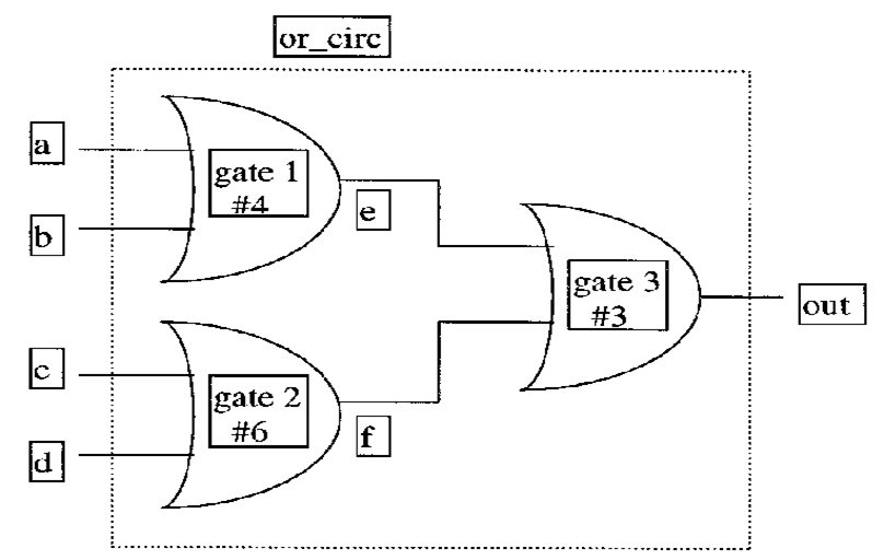
The gate function and delay, for example for gate 1, can be described in the following manner:
or #4 a1 (e, a, b);
A delay of 4 is assigned to the or-gate. This means that the output of the gate, e, is delayed by 4 from the inputs a and b.
The module explaining Figure 1 can be of two forms:
1)
The above or_circ modules results in delays of (4+3) = 7 and (6+3) = 9 for the 4 connections part from the input to the output of the circuit.
Lumped Delay
Lumped delay is delay assigned as a single delay in each module, mostly to the output gate of the module. The cumulative delay of all paths is lumped at one location. The figure below is an example of lumped delay. This figure is similar as the figure of the distributed delay, but with the sum delay of the longest path assigned to the output gate: (delay of gate 2 + delay of gate 3) = 9.

The program corresponding to Figure 2, is very similar to the one for distributed delay. The difference is that only or - gate 3 has got a delay assigned to it:
1)
Pin - to Pin Delay
Pin - to - Pin delay, also called path delay, is delay assigned to paths from each input to each output. An example circuit is shown below.
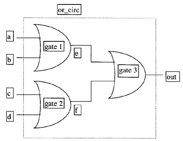
path a - e - out, delay = 7
The module for the above circuit is shown beneath:
Module or_circ (out, a, b, c, d);
For larger circuits, the pin - to - pin delay can be easier to model than distributed delay. This is because the designer writing delay models, needs to know only the input / output pins of the module, rather than the internals of the module. The path delays for digital circuits can be found through different simulation programs, for instance SPICE. Pin - to - Pin delays for standard parts can be found from data books. By using the path delay model, the program speed will increase.
8) Tell something about delay modeling timing checks?
Delay Modeling: Timing Checks.
Keywords: $setup, $hold, $width
This section, the final part of the delay modeling chapter, discusses some of the various system tasks that exist for the purposes of timing checks. Verilog contains many timing-check system tasks, but only the three most common tasks are discussed here: $setup, $hold and $width. Timing checks are used to verify that timing constraints are upheld, and are especially important in the simulation of high-speed sequential circuits such as microprocessors. All timing checks must be contained within specify blocks as shown in the example below.
The $setup and $hold tasks are used to monitor the setup and hold constraints during the simulation of a sequential circuit element. In the example, the setup time is the minimum allowed time between a change in the input d and a positive clock edge. Similarly, the hold time is the minimum allowed time between a positive clock edge and a change in the input d.
The $width task is used to check the minimum width of a positive or negative-going pulse. In the example, this is the time between a negative transition and the transition back to 1.

Syntax:
NB: data_change, reference and reference1 must be declared wires.
$setup(data_change, reference, time_limit);
data_change: signal that is checked against the reference
reference: signal used as reference
time_limit: minimum time required between the two events.
Violation if: Treference - Tdata_change < time_limit.
$hold(reference, data_change, time_limit);
reference: signal used as reference
data_change: signal that is checked against the reference
time_limit: minimum time required between the two events.
Violation if: Tdata_change - Treference < time_limit
$width(reference1, time_limit);
reference1: first transition of signal
time_limit: minimum time required between transition1 and transition2.
Violation if: Treference2 - Treference1 < time_limit
Example:
Output:
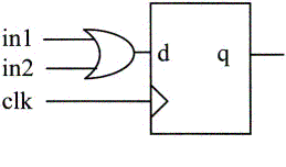
9) Draw a 2:1 mux using switches and verilog code for it?
1-bit 2-1 Multiplexer
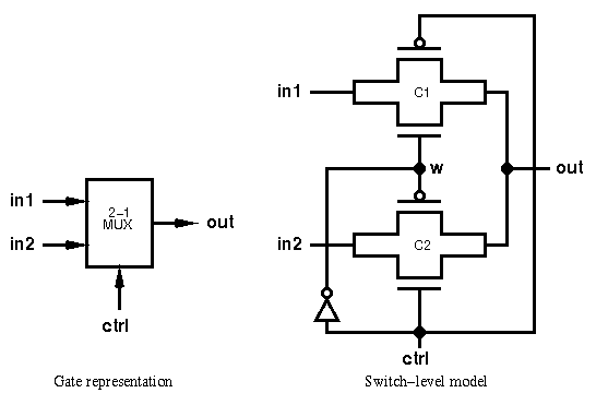 This circuit assigns the output out to either inputs in1 or in2 depending on the low or high values of ctrl respectively.
Two transmission gates, of instance names C1 and C2, are implemented with the cmos statement, in the format
10)What are the synthesizable gate level constructs?

The above table gives all the gate level constructs of only the constructs in first two columns are synthesizable.
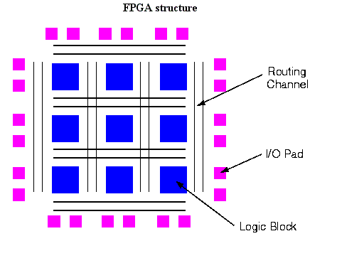
A field-programmable gate array is a semiconductor device containing programmable logic components called "logic blocks", and programmable interconnects. Logic blocks can be programmed to perform the function of basic logic gates such as AND, and XOR, or more complex combinational functions such as decoders or mathematical functions. In most FPGAs, the logic blocks also include memory elements, which may be simple flip-flops or more complete blocks of memory. A hierarchy of programmable interconnects allows logic blocks to be interconnected as needed by the system designer, somewhat like a one-chip programmable breadboard. Logic blocks and interconnects can be programmed by the customer or designer, after the FPGA is manufactured, to implement any logical function—hence the name "field-programmable". FPGAs are usually slower than their application-specific integrated circuit (ASIC) counterparts, cannot handle as complex a design, and draw more power (for any given semiconductor process). But their advantages include a shorter time to market, ability to re-program in the field to fix bugs, and lower non-recurring engineering costs. Vendors can sell cheaper, less flexible versions of their FPGAs which cannot be modified after the design is committed. The designs are developed on regular FPGAs and then migrated into a fixed version that more resembles an ASIC.
What logic is inferred when there are multiple assign statements targeting the same wire?
It is illegal to specify multiple assign statements to the same wire in a synthesizable code that will become an output port of the module. The synthesis tools give a syntax error that a net is being driven by more than one source.
However, it is legal to drive a three-state wire by multiple assign statements.
What do conditional assignments get inferred into?
Conditionals in a continuous assignment are specified through the “?:” operator. Conditionals get inferred into a multiplexor. For example, the following is the code for a simple multiplexor
assign wire1 = (sel==1'b1) ? a : b;

What value is inferred when multiple procedural assignments made to the same reg variable in an always block?
When there are multiple nonblocking assignments made to the same reg variable in a sequential always block, then the last assignment is picked up for logic synthesis. For example
always @ (posedge clk) begin
out <= in1^in2;
out <= in1 &in2;
out <= in1|in2;
In the example just shown, it is the OR logic that is the last assignment. Hence, the logic synthesized was indeed the OR gate. Had the last assignment been the “&” operator, it would have synthesized an AND gate.
1) What is minimum and maximum frequency of dcm in spartan-3 series fpga?
Spartan series dcm’s have a minimum frequency of 24 MHZ and a maximum of 248
2)Tell me some of constraints you used and their purpose during your design?
There are lot of constraints and will vary for tool to tool ,I am listing some of Xilinx constraints
a) Translate on and Translate off: the Verilog code between Translate on and Translate off is ignored for synthesis.
b) CLOCK_SIGNAL: is a synthesis constraint. In the case where a clock signal goes through combinatorial logic before being connected to the clock input of a flip-flop, XST cannot identify what input pin or internal net is the real clock signal. This constraint allows you to define the clock net.
c) XOR_COLLAPSE: is synthesis constraint. It controls whether cascaded XORs should be collapsed into a single XOR.
For more constraints detailed description refer to constraint guide.
3) Suppose for a piece of code equivalent gate count is 600 and for another code equivalent gate count is 50,000 will the size of bitmap change?in other words will size of bitmap change it gate count change?
The size of bitmap is irrespective of resource utilization, it is always the same,for Spartan xc3s5000 it is 1.56MB and will never change.
4) What are different types of FPGA programming modes?what are you currently using ?how to change from one to another?
Before powering on the FPGA, configuration data is stored externally in a PROM or some other nonvolatile medium either on or off the board. After applying power, the configuration data is written to the FPGA using any of five different modes: Master Parallel, Slave Parallel, Master Serial, Slave Serial, and Boundary Scan (JTAG). The Master and Slave Parallel modes
Mode selecting pins can be set to select the mode, refer data sheet for further details.
5) Tell me some of features of FPGA you are currently using?
I am taking example of xc3s5000 to answering the question .
Very low cost, high-performance logic solution for
high-volume, consumer-oriented applications
- Densities as high as 74,880 logic cells
- Up to 784 I/O pins
- 622 Mb/s data transfer rate per I/O
- 18 single-ended signal standards
- 6 differential I/O standards including LVDS, RSDS
- Termination by Digitally Controlled Impedance
- Signal swing ranging from 1.14V to 3.45V
- Double Data Rate (DDR) support
• Logic resources
- Abundant logic cells with shift register capability
- Wide multiplexers
- Fast look-ahead carry logic
- Dedicated 18 x 18 multipliers
- Up to 1,872 Kbits of total block RAM
- Up to 520 Kbits of total distributed RAM
• Digital Clock Manager (up to four DCMs)
- Clock skew elimination
• Eight global clock lines and abundant routing
6) What is gate count of your project?
Well mine was 3.2 million, I don’t know yours.!
7) Can you list out some of synthesizable and non synthesizable constructs?
not synthesizable->>>>
initial
ignored for synthesis.
delays
ignored for synthesis.
events
not supported.
real
Real data type not supported.
time
Time data type not supported.
force and release
Force and release of data types not supported.
fork join
Use nonblocking assignments to get same effect.
user defined primitives
Only gate level primitives are supported.
synthesizable constructs->>
assign,for loop,Gate Level Primitives,repeat with constant value...
8)Can you explain what struck at zero means?
These stuck-at problems will appear in ASIC. Some times, the nodes will permanently tie to 1 or 0 because of some fault. To avoid that, we need to provide testability in RTL. If it is permanently 1 it is called stuck-at-1 If it is permanently 0 it is called stuck-at-0.
9) Can you draw general structure of fpga?
10) Difference between FPGA and CPLD?
FPGA:
a)SRAM based technology.
b)Segmented connection between elements.
c)Usually used for complex logic circuits.
d)Must be reprogrammed once the power is off.
e)Costly
CPLD:
a)Flash or EPROM based technology.
b)Continuous connection between elements.
c)Usually used for simpler or moderately complex logic circuits.
d)Need not be reprogrammed once the power is off.
e)Cheaper
11) What are dcm's?why they are used?
Digital clock manager (DCM) is a fully digital control system that
uses feedback to maintain clock signal characteristics with a
high degree of precision despite normal variations in operating
temperature and voltage.
That is clock output of DCM is stable over wide range of temperature and voltage , and also skew associated with DCM is minimal and all phases of input clock can be obtained . The output of DCM coming form global buffer can handle more load.
12) FPGA design flow?

Also,Please refer to presentation section synthesis ppt on this site.
13)what is slice,clb,lut?
I am taking example of xc3s500 to answer this question
The Configurable Logic Blocks (CLBs) constitute the main logic resource for implementing synchronous as well as combinatorial circuits.
CLB are configurable logic blocks and can be configured to combo,ram or rom depending on coding style
CLB consist of 4 slices and each slice consist of two 4-input LUT (look up table) F-LUT and G-LUT.
14) Can a clb configured as ram?
YES.
The memory assignment is a clocked behavioral assignment, Reads from the memory are asynchronous, And all the address lines are shared by the read and write statements.
15)What is purpose of a constraint file what is its extension?
The UCF file is an ASCII file specifying constraints on the logical design. You create this file and enter your constraints in the file with a text editor. You can also use the Xilinx Constraints Editor to create constraints within a UCF(extention) file. These constraints affect how the logical design is implemented in the target device. You can use the file to override constraints specified during design entry.
16) What is FPGA you are currently using and some of main reasons for choosing it?
17) Draw a rough diagram of how clock is routed through out FPGA?

18) How many global buffers are there in your current fpga,what is their significance?
There are 8 of them in xc3s5000
An external clock source enters the FPGA using a Global Clock Input Buffer (IBUFG), which directly accesses the global clock network or an Input Buffer (IBUF). Clock signals within the FPGA drive a global clock net using a Global Clock Multiplexer Buffer (BUFGMUX). The global clock net connects directly to the CLKIN input.
19) What is frequency of operation and equivalent gate count of u r project?
20)Tell me some of timing constraints you have used?
21)Why is map-timing option used?
Timing-driven packing and placement is recommended to improve design performance, timing, and packing for highly utilized designs.
22)What are different types of timing verifications?
Dynamic timing:
a. The design is simulated in full timing mode.
b. Not all possibilities tested as it is dependent on the input test vectors.
c. Simulations in full timing mode are slow and require a lot of memory.
d. Best method to check asynchronous interfaces or interfaces between different timing domains.
Static timing:
a. The delays over all paths are added up.
b. All possibilities, including false paths, verified without the need for test vectors.
c. Much faster than simulations, hours as opposed to days.
d. Not good with asynchronous interfaces or interfaces between different timing domains.
23) Compare PLL & DLL ?
PLL:
PLLs have disadvantages that make their use in high-speed designs problematic, particularly when both high performance and high reliability are required.
The PLL voltage-controlled oscillator (VCO) is the greatest source of problems. Variations in temperature, supply voltage, and manufacturing process affect the stability and operating performance of PLLs.
DLLs, however, are immune to these problems. A DLL in its simplest form inserts a variable delay line between the external clock and the internal clock. The clock tree distributes the clock to all registers and then back to the feedback pin of the DLL.
The control circuit of the DLL adjusts the delays so that the rising edges of the feedback clock align with the input clock. Once the edges of the clocks are aligned, the DLL is locked, and both the input buffer delay and the clock skew are reduced to zero.
Advantages:
· precision
· stability
· power management
· noise sensitivity
· jitter performance.
24) Given two ASICs. one has setup violation and the other has hold violation. how can they be made to work together without modifying the design?
Slow the clock down on the one with setup violations..
And add redundant logic in the path where you have hold violations.
25)Suggest some ways to increase clock frequency?
· Check critical path and optimize it.
· Add more timing constraints (over constrain).
· pipeline the architecture to the max possible extent keeping in mind latency req's.
26)What is the purpose of DRC?
DRC is used to check whether the particular schematic and corresponding layout(especially the mask sets involved) cater to a pre-defined rule set depending on the technology used to design. They are parameters set aside by the concerned semiconductor manufacturer with respect to how the masks should be placed , connected , routed keeping in mind that variations in the fab process does not effect normal functionality. It usually denotes the minimum allowable configuration.
27)What is LVs and why do we do that. What is the difference between LVS and DRC?
The layout must be drawn according to certain strict design rules. DRC helps in layout of the designs by checking if the layout is abide by those rules.
After the layout is complete we extract the netlist. LVS compares the netlist extracted from the layout with the schematic to ensure that the layout is an identical match to the cell schematic.
28)What is DFT ?
DFT means design for testability. 'Design for Test or Testability' - a methodology that ensures a design works properly after manufacturing, which later facilitates the failure analysis and false product/piece detection
Other than the functional logic,you need to add some DFT logic in your design.This will help you in testing the chip for manufacturing defects after it come from fab. Scan,MBIST,LBIST,IDDQ testing etc are all part of this. (this is a hot field and with lots of opportunities)
29) There are two major FPGA companies: Xilinx and Altera. Xilinx tends to promote its hard processor cores and Altera tends to promote its soft processor cores. What is the difference between a hard processor core and a soft processor core?
A hard processor core is a pre-designed block that is embedded onto the device. In the Xilinx Virtex II-Pro, some of the logic blocks have been removed, and the space that was used for these logic blocks is used to implement a processor. The Altera Nios, on the other hand, is a design that can be compiled to the normal FPGA logic.
30)What is the significance of contamination delay in sequential circuit timing?
Look at the figure below. tcd is the contamination delay.

Contamination delay tells you if you meet the hold time of a flip flop. To understand this better please look at the sequential circuit below.

The contamination delay of the data path in a sequential circuit is critical for the hold time at the flip flop where it is exiting, in this case R2.
mathematically, th(R2) <= tcd(R1) + tcd(CL2)
Contamination delay is also called tmin and Propagation delay is also called tmax in many data sheets.
31)When are DFT and Formal verification used?
DFT:
· manufacturing defects like stuck at "0" or "1".
· test for set of rules followed during the initial design stage.
Formal verification:
· Verification of the operation of the design, i.e, to see if the design follows spec.
· gate netlist == RTL ?
· using mathematics and statistical analysis to check for equivalence.
32)What is Synthesis?
Synthesis is the stage in the design flow which is concerned with translating your Verilog code into gates - and that's putting it very simply! First of all, the Verilog must be written in a particular way for the synthesis tool that you are using. Of course, a synthesis tool doesn't actually produce gates - it will output a netlist of the design that you have synthesised that represents the chip which can be fabricated through an ASIC or FPGA vendor.
33)We need to sample an input or output something at different rates, but I need to vary the rate? What's a clean way to do this?
Many, many problems have this sort of variable rate requirement, yet we are usually constrained with a constant clock frequency. One trick is to implement a digital NCO (Numerically Controlled Oscillator). An NCO is actually very simple and, while it is most naturally understood as hardware, it also can be constructed in software. The NCO, quite simply, is an accumulator where you keep adding a fixed value on every clock (e.g. at a constant clock frequency). When the NCO "wraps", you sample your input or do your action. By adjusting the value added to the accumulator each clock, you finely tune the AVERAGE frequency of that wrap event. Now - you may have realized that the wrapping event may have lots of jitter on it. True, but you may use the wrap to increment yet another counter where each additional Divide-by-2 bit reduces this jitter. The DDS is a related technique. I have two examples showing both an NCOs and a DDS in my File Archive. This is tricky to grasp at first, but tremendously powerful once you have it in your bag of tricks. NCOs also relate to digital PLLs, Timing Recovery, TDMA and other "variable rate" phenomena


How to write FSM is verilog?
there r mainly 4 ways 2 write fsm code
1) using 1 process where all input decoder, present state, and output decoder r combine in one process.
2) using 2 process where all comb ckt and sequential ckt separated in different process
3) using 2 process where input decoder and persent state r combine and output decoder seperated in other process
4) using 3 process where all three, input decoder, present state and output decoder r separated in 3 process.
(Also refer to Tutorial section for more)
Verilog interview Questions
21)What is difference between freeze deposit and force?
$deposit(variable, value);
This system task sets a Verilog register or net to the specified value. variable is the
register or net to be changed; value is the new value for the register or net. The value
remains until there is a subsequent driver transaction or another $deposit task for the
same register or net. This system task operates identically to the ModelSim
force -deposit command.
The force command has -freeze, -drive, and -deposit options. When none of these is
specified, then -freeze is assumed for unresolved signals and -drive is assumed for resolved
signals. This is designed to provide compatibility with force files. But if you prefer -freeze
as the default for both resolved and unresolved signals.
Verilog interview Questions
22)Will case infer priority register if yes how give an example?
yes case can infer priority register depending on coding style
reg r;
// Priority encoded mux,
always @ (a or b or c or select2)
begin
r = c;
case (select2)
2'b00: r = a;
2'b01: r = b;
endcase
end
Verilog interview Questions
23)Casex,z difference,which is preferable,why?
CASEZ :
Special version of the case statement which uses a Z logic value to represent don't-care bits. CASEX :
Special version of the case statement which uses Z or X logic values to represent don't-care bits.
CASEZ should be used for case statements with wildcard don’t cares, otherwise use of CASE is required; CASEX should never be used.
This is because:
Don’t cares are not allowed in the "case" statement. Therefore casex or casez are required. Casex will automatically match any x or z with anything in the case statement. Casez will only match z’s -- x’s require an absolute match.
Verilog interview Questions
24)Given the following Verilog code, what value of "a" is displayed?
always @(clk) begin
a = 0;
a <= 1;
$display(a);
end
This is a tricky one! Verilog scheduling semantics basically imply a
four-level deep queue for the current simulation time:
1: Active Events (blocking statements)
2: Inactive Events (#0 delays, etc)
3: Non-Blocking Assign Updates (non-blocking statements)
4: Monitor Events ($display, $monitor, etc).
Since the "a = 0" is an active event, it is scheduled into the 1st "queue".
The "a <= 1" is a non-blocking event, so it's placed into the 3rd queue.
Finally, the display statement is placed into the 4th queue. Only events in the active queue are completed this sim cycle, so the "a = 0" happens, and then the display shows a = 0. If we were to look at the value of a in the next sim cycle, it would show 1.
25) What is the difference between the following two lines of Verilog code?
#5 a = b;
a = #5 b;
#5 a = b; Wait five time units before doing the action for "a = b;".
a = #5 b; The value of b is calculated and stored in an internal temp register,After five time units, assign this stored value to a.
26)What is the difference between:
c = foo ? a : b;
and
if (foo) c = a;
else c = b;
The ? merges answers if the condition is "x", so for instance if foo = 1'bx, a = 'b10, and b = 'b11, you'd get c = 'b1x. On the other hand, if treats Xs or Zs as FALSE, so you'd always get c = b.
27)What are Intertial and Transport Delays ??
28)What does `timescale 1 ns/ 1 ps signify in a verilog code?
'timescale directive is a compiler directive.It is used to measure simulation time or delay time. Usage : `timescale
29) What is the difference between === and == ?
output of "==" can be 1, 0 or X.
output of "===" can only be 0 or 1.
When you are comparing 2 nos using "==" and if one/both the numbers have one or more bits as "x" then the output would be "X" . But if use "===" outpout would be 0 or 1.
e.g A = 3'b1x0
B = 3'b10x
A == B will give X as output.
A === B will give 0 as output.
"==" is used for comparison of only 1's and 0's .It can't compare Xs. If any bit of the input is X output will be X
"===" is used for comparison of X also.
30)How to generate sine wav using verilog coding style?
A: The easiest and efficient way to generate sine wave is using CORDIC Algorithm.
31) What is the difference between wire and reg?
Net types: (wire,tri)Physical connection between structural elements. Value assigned by a continuous assignment or a gate output. Register type: (reg, integer, time, real, real time) represents abstract data storage element. Assigned values only within an always statement or an initial statement. The main difference between wire and reg is wire cannot hold (store) the value when there no connection between a and b like a->b, if there is no connection in a and b, wire loose value. But reg can hold the value even if there in no connection. Default values:wire is Z,reg is x.
32 )How do you implement the bi-directional ports in Verilog HDL?
module bidirec (oe, clk, inp, outp, bidir);
// Port Declaration
input oe;
input clk;
input [7:0] inp;
output [7:0] outp;
inout [7:0] bidir;
reg [7:0] a;
reg [7:0] b;
assign bidir = oe ? a : 8'bZ ;
assign outp = b;
// Always Construct
always @ (posedge clk)
begin
b <= bidir;
a <= inp;
end
endmodule
34)what is verilog case (1) ?
wire [3:0] x;
always @(...) begin
case (1'b1)
x[0]: SOMETHING1;
x[1]: SOMETHING2;
x[2]: SOMETHING3;
x[3]: SOMETHING4;
endcase
end
The case statement walks down the list of cases and executes the first one that matches. So here, if the lowest 1-bit of x is bit 2, then something3 is the statement that will get executed (or selected by the logic).
35) Why is it that "if (2'b01 & 2'b10)..." doesn't run the true case?
This is a popular coding error. You used the bit wise AND operator (&) where you meant to use the logical AND operator (&&).
36)What are Different types of Verilog Simulators ?
There are mainly two types of simulators available.
Event Driven
Cycle Based
Event-based Simulator:
This Digital Logic Simulation method sacrifices performance for rich functionality: every active signal is calculated for every device it propagates through during a clock cycle. Full Event-based simulators support 4-28 states; simulation of Behavioral HDL, RTL HDL, gate, and transistor representations; full timing calculations for all devices; and the full HDL standard. Event-based simulators are like a Swiss Army knife with many different features but none are particularly fast.
Cycle Based Simulator:
This is a Digital Logic Simulation method that eliminates unnecessary calculations to achieve huge performance gains in verifying Boolean logic:
1.) Results are only examined at the end of every clock cycle; and
2.) The digital logic is the only part of the design simulated (no timing calculations). By limiting the calculations, Cycle based Simulators can provide huge increases in performance over conventional Event-based simulators.
Cycle based simulators are more like a high speed electric carving knife in comparison because they focus on a subset of the biggest problem: logic verification.
Cycle based simulators are almost invariably used along with Static Timing verifier to compensate for the lost timing information coverage.
37)What is Constrained-Random Verification ?
Introduction
As ASIC and system-on-chip (SoC) designs continue to increase in size and complexity, there is an equal or greater increase in the size of the verification effort required to achieve functional coverage goals. This has created a trend in RTL verification techniques to employ constrained-random verification, which shifts the emphasis from hand-authored tests to utilization of compute resources. With the corresponding emergence of faster, more complex bus standards to handle the massive volume of data traffic there has also been a renewed significance for verification IP to speed the time taken to develop advanced testbench environments that include randomization of bus traffic.
Directed-Test Methodology
Building a directed verification environment with a comprehensive set of directed tests is extremely time-consuming and difficult. Since directed tests only cover conditions that have been anticipated by the verification team, they do a poor job of covering corner cases. This can lead to costly re-spins or, worse still, missed market windows.
Traditionally verification IP works in a directed-test environment by acting on specific testbench commands such as read, write or burst to generate transactions for whichever protocol is being tested. This directed traffic is used to verify that an interface behaves as expected in response to valid transactions and error conditions. The drawback is that, in this directed methodology, the task of writing the command code and checking the responses across the full breadth of a protocol is an overwhelming task. The verification team frequently runs out of time before a mandated tape-out date, leading to poorly tested interfaces. However, the bigger issue is that directed tests only test for predicted behavior and it is typically the unforeseen that trips up design teams and leads to extremely costly bugs found in silicon.
Constrained-Random Verification Methodology
The advent of constrained-random verification gives verification engineers an effective method to achieve coverage goals faster and also help find corner-case problems. It shifts the emphasis from writing an enormous number of directed tests to writing a smaller set of constrained-random scenarios that let the compute resources do the work. Coverage goals are achieved not by the sheer weight of manual labor required to hand-write directed tests but by the number of processors that can be utilized to run random seeds. This significantly reduces the time required to achieve the coverage goals.
Scoreboards are used to verify that data has successfully reached its destination, while monitors snoop the interfaces to provide coverage information. New or revised constraints focus verification on the uncovered parts of the design under test. As verification progresses, the simulation tool identifies the best seeds, which are then retained as regression tests to create a set of scenarios, constraints, and seeds that provide high coverage of the design.
What are the differences between blocking and nonblocking assignments?
While both blocking and nonblocking assignments are procedural assignments, they differ in behaviour with respect to simulation and logic
synthesis as follows:
How can I model a bi-directional net with assignments influencing both source and destination?
The assign statement constitutes a continuous assignment. The changes on the RHS of the statement immediately reflect on the LHS net. However, any changes on the LHS don't get reflected on the RHS. For example, in the following statement, changes to the rhs net will update the lhs net, but not vice versa.
System Verilog has introduced a keyword alias, which can be used only on nets to have a two-way assignment. For example, in the following code, any changes to the rhs is reflected to the lh s , and vice versa.
wire rhs , lhs
assign lhs=rhs;
System Verilog has introduced a keyword alias, which can be used only on nets to have a two-way assignment. For example, in the following code, any changes to the rhs is reflected to the lh s , and vice versa.
module test ();
wire rhs,lhs;
alias lhs=rhs;
In the above example, any change to either side of the net gets reflected on the other side.
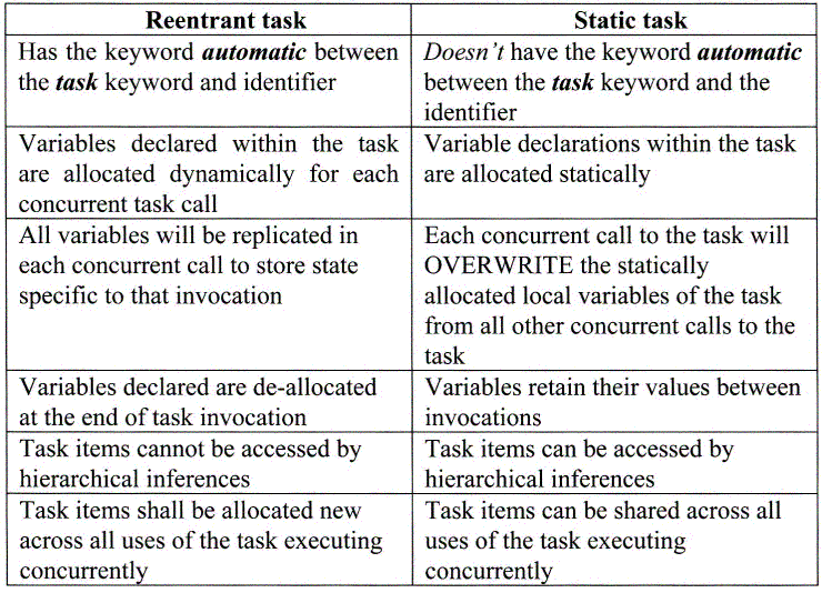
Are tasks and functions re-entrant, and how are they different from static task and function calls?
In Verilog-95, tasks and functions were not re-entrant. From Verilog version 2001 onwards, the tasks and functions are reentrant. The reentrant tasks have a keyword automatic between the keyword task and the name of the task. The presence of the keyword automatic replicates and allocates the variables within a task dynamically for each task entry during concurrent task calls, i.e., the values don’t get overwritten for each task call. Without the keyword, the variables are allocated statically, which means these variables are shared across different task calls, and can hence get overwritten by each task call.
How can I override variables in an automatic task?
By default, all variables in a module are static, i.e., these variables will be replicated for all instances of a module. However, in the case of task and function, either the task/function itself or the variables within them can be defined as static or automatic. The following explains the inferences through different combinations of the task/function and/or its variables, declared either as static or automatic:
No automatic definition of task/function or its variables This is the Verilog-1995 format, wherein the task/function and its variables were implicitly static. The variables are allocated only once. Without the mention of the automatic keyword, multiple calls to task/function will override their variables.
static task/function definition
System Verilog introduced the keyword static. When a task/function is explicitly defined as static, then its variables are allocated only once, and can be overridden. This scenario is exactly the same scenario as before.
automatic task/function definition
From Verilog-2001 onwards, and included within SystemVerilog, when the task/function is declared as automatic, its variables are also implicitly automatic. Hence, during multiple calls of the task/function, the variables are allocated each time and replicated without any overwrites.
static task/function and automatic variables
SystemVerilog also allows the use of automatic variables in a static task/function. Those without any changes to automatic variables will remain implicitly static. This will be useful in scenarios wherein the implicit static variables need to be initialised before the task call, and the automatic variables can be allocated each time.
automatic task/function and static variables
SystemVerilog also allows the use of static variables in an automatic task/function. Those without any changes to static variables will remain implicitly automatic. This will be useful in scenarios wherein the static variables need to be updated for each call, whereas the rest can be allocated each time.
What are the rules governing usage of a Verilog function?
The following rules govern the usage of a Verilog function construct:A function cannot advance simulation-time, using constructs like #, @. etc.
A function shall not have nonblocking assignments.
A function without a range defaults to a one bit reg for the return value.
It is illegal to declare another object with the same name as the function in the scope where the function is declared.
How do I prevent selected parameters of a module from being overridden during instantiation?
If a particular parameter within a module should be prevented from being overridden, then it should be declared using the localparam construct, rather than the parameter construct. The localparam construct has been introduced from Verilog-2001. Note that a localparam variable is fully identical to being defined as a parameter, too. In the following example, the localparam construct is used to specify num_bits, and hence trying to override it directly gives an error message.Note, however, that, since the width and depth are specified using the parameter construct, they can be overridden during instantiation or using defparam, and hence will indirectly override the num_bits values. In general, localparam constructs are useful in defining new and localized identifiers whose values are derived from regular parameters.
What are the pros and cons of specifying the parameters using the defparam construct vs. specifying during instantiation?
The advantages of specifying parameters during instantiation method are:
All the values to all the parameters don’t need to be specified. Only those parameters that are assigned the new values need to be specified. The unspecified parameters will retain their default values specified within its module definition.
The order of specifying the parameter is not relevant anymore, since the parameters are directly specified and linked by their name.
The disadvantage of specifying parameter during instantiation are:
This has a lower precedence when compared to assigning using defparam.
The advantages of specifying parameter assignments using defparam are:
This method always has precedence over specifying parameters during instantiation.
All the parameter value override assignments can be grouped inside one module and together in one place, typically in the top-level testbench itself.
When multiple defparams for a single parameter are specified, the parameter takes the value of the last defparam statement encountered in the source if, and only if, the multiple defparam’s are in the same file. If there are defparam’s in different files that override the same parameter, the final value of the parameter is indeterminate.
The disadvantages of specifying parameter assignments using defparam are:
The parameter is typically specified by the scope of the hierarchies underneath which it exists. If a particular module gets ungrouped in its hierarchy, [sometimes necessary during synthesis], then the scope to specify the parameter is lost, and is unspecified. B
For example, if a module is instantiated in a simulation testbench, and its internal parameters are then overridden using hierarchical defparam constructs (For example, defparam U1.U_fifo.width = 32;). Later, when this module is synthesized, the internal hierarchy within U1 may no longer exist in the gate-level netlist, depending upon the synthesis strategy chosen. Therefore post-synthesis simulation will fail on the hierarchical defparam override.
Can there be full or partial no-connects to a multi-bit port of a module during its instantiation?
No. There cannot be full or partial no-connects to a multi-bit port of a module during instantiationWhat happens to the logic after synthesis, that is driving an unconnected output port that is left open (, that is, noconnect) during its module instantiation?
An unconnected output port in simulation will drive a value, but this value does not propagate to any other logic. In synthesis, the cone of any combinatorial logic that drives the unconnected output will get optimized away during boundary optimisation, that is, optimization by synthesis tools across hierarchical boundaries.How is the connectivity established in Verilog when connecting wires of different widths?
When connecting wires or ports of different widths, the connections are right-justified, that is, the rightmost bit on the RHS gets connected to the rightmost bit of the LHS and so on, until the MSB of either of the net is reached.Can I use a Verilog function to define the width of a multi-bit port, wire, or reg type?
The width elements of ports, wire or reg declarations require a constant in both MSB and LSB. Before Verilog 2001, it is a syntax error to specify a function call to evaluate the value of these widths. For example, the following code is erroneous before Verilog 2001 version.reg [ port1(val1:vla2) : port2 (val3:val4)] reg1;
In the above example, get_high and get_low are both function calls of evaluating a constant result for MSB and LSB respectively. However, Verilog-2001 allows the use of a function call to evaluate the MSB or LSB of a width declaration
What is the implication of a combinatorial feedback loops in design testability?
The presence of feedback loops should be avoided at any stage of the design, by periodically checking for it, using the lint or synthesis tools. The presence of the feedback loop causes races and hazards in the design, and 104 RTL Designleads to unpredictable logic behavior. Since the loops are delay-dependent, they cannot be tested with any ATPG algorithm. Hence, combinatorial loops should be avoided in the logic.
What are the various methods to contain power during RTL coding?
Any switching activity in a CMOS circuit creates a momentary current flow from VDD to GND during logic transition, when both N and P type transistors are ON, and, hence, increases power consumption.The most common storage element in the designs being the synchronous FF, its output can change whenever its data input toggles, and the clock triggers. Hence, if these two elements can be asserted in a controlled fashion, so that the data is presented to the D input of the FF only when required, and the clock is also triggered only when required, then it will reduce the switching activity, and, automatically the power.
The following bullets summarize a few mechanisms to reduce the power consumption:
How do I model Analog and Mixed-Signal blocks in Verilog?
First, this is a big area.Analog and Mixed-Signal designers use tools like Spice to fully characterize and model their designs.My only involvement with Mixed-Signal blocks has been to utilize behavioral models of things like PLLs, A/Ds, D/As within a larger SoC.There are some specific Verilog tricks to this which is what this FAQ is about (I do not wish to trivialize true Mixed-Signal methodology, but us chip-level folks need to know this trick).
A mixed-signal behavioral model might model the digital and analog input/output behavior of, for example, a D/A (Digital to Analog Converter).So, digital input in and analog voltage out.Things to model might be the timing (say, the D/A utilizes an internal Success Approximation algorithm), output range based on power supply voltages, voltage biases, etc.A behavioral model may not have any knowledge of the physical layout and therefore may not offer any fidelity whatsoever in terms of noise, interface, cross-talk, etc.A model might be parameterized given a specific characterization for a block.Be very careful about the assumptions and limitations of the model!
Issue #1; how do we model analog voltages in Verilog.Answer: use the Verilog real data type, declare “analog wires” as wire[63:0] in order to use a 64-bit floating-type represenation, and use the built-in PLI functions:
$rtoi converts reals to integers w/truncation e.g. 123.45 -> 123
$itor converts integers to reals e.g. 123 -> 123.0
$realtobits converts reals to 64-bit vector
$bitstoreal converts bit pattern to real
That was a lot.This is a trick to be used in vanilla Verilog.The 64-bit wire is simply a ways to actually interface to the ports of the mixed-signal block.In other words, our example D/A module may have an output called AOUT which is a voltage.Verilog does not allow us to declare an output port of type REAL.So, instead declare AOUT like this:
module dtoa (clk, reset..... aout.....);
....
wire [63:0]aout;// Analog output
....
We use 64 bits because we can use floating-point numbers to represent out voltage output (e.g. 1.22x10⁻³ for 1.22 millivolts).The floating-point value is relevant only to Verilog and your workstation and processor, and the IEEE floating-point format has NOTHING to do with the D/A implementation.Note the disconnect in terms of the netlist itself.The physical “netlist” that you might see in GDS may have a single metal interconnect that is AOUT, and obviously NOT 64 metal wires.Again, this is a trick.The 64-bit bus is only for wiring.You may have to do some quick netlist substitutions when you hand off a netlist.
In Verilog, the real data type is basically a floating-point number (e.g. like double in C).If you want to model an analog value either within the mixed-signal behavorial model, or externally in the system testbench (e.g. the sensor or actuator), use the real data type.You can convert back and forth between real and your wire [63:0] using the PLI functions listed above.A trivial D/A model could simply take the digital input value, convert it to real, scale it according to some #defines, and output the value on AOUT as the 64-bit “psuedo-analog” value.Your testbench can then do the reverse and print out the value, or whatever.More sophisticated models can model the Successive Approximation algorithm, employ look-ups, equations, etc. etc.
That’s it.If you are getting a mixed-signal block from a vendor, then you may also receive (or you should ask for) the behavioral Verilog models for the IP.
How do I synthesize Verilog into gates with Synopsys?
The answer can, of course, occupy several lifetimes to completely answer.. BUT.. a straight-forward Verilog module can be very easily synthesized using Design Compiler (e.g. dc_shell). Most ASIC projects will create very elaborate synthesis scripts, CSH scripts, Makefiles, etc. This is all important in order automate the process and generalize the synthesis methodology for an ASIC project or an organization. BUT don't let this stop you from creating your own simple dc_shell experiments!
Let's say you create a Verilog module named foo.v that has a single clock input named 'clk'. You want to synthesize it so that you know it is synthesizable, know how big it is, how fast it is, etc. etc. Try this:
target_library = { CORELIB.db } <--- This part you need to get from your vendor...
read -format verilog foo.v
create_clock -name clk -period 37.0
set_clock_skew -uncertainty 0.4 clk
set_input_delay 1.0 -clock clk all_inputs() - clk - reset
set_output_delay 1.0 -clock clk all_outputs()
compile
report_area
report_timing
write -format db -hierarchy -output foo.db
write -format verilog -hierarchy -output foo.vg
quit
You can enter all this in interactively, or put it into a file called 'synth_foo.scr' and then enter:dc_shell -f synth_foo.scr
You can spend your life learning more and more Synopsys and synthesis-related commands and techniques, but don't be afraid to begin using these simple commands.How can I pass parameters to my simulation?
A testbench and simulation will likely need many different parameters and settings for different sorts of tests and conditions. It is definitely a good idea to concentrate on a single testbench file that is parameterized, rather than create a dozen seperate, yet nearly identical, testbenches. Here are 3 common techniques:
· Use a define. This is almost exactly the same approach as the #define and -D compiler arg that C programs use. In your Verilog code, use a `define to define the variable condition and then use the Verilog preprocessor directives like `ifdef. Use the '+define+' Verilog command line option. For example:
... to run the simulation ..
verilog testbench.v cpu.v +define+USEWCSDF
... in your code ...
`ifdef USEWCSDF
initial $sdf_annotate (testbench.cpu, "cpuwc.sdf");
`endif
The +define+ can also be filled in from your Makefile invocation, which in turn, can be finally
filled in the your UNIX promp command line.
Defines are a blunt weapon because they are very global and you can only do so much with
them since they are a pre-processor trick. Consider the next approach before resorting to
defines.
· Use parameters and parameter definition modules. Parameters are not preprocessor definitions and they have scope (e.g. parameters are associated with specific modules). Parameters are therefore more clean, and if you are in the habit of using a lot of defines; consider switching to parameters. As an example, lets say we have a test (e.g. test12) which needs many parameters to have particular settings. In your code, you might have this sort of stuff:
module testbench_uart1 (....)
parameter BAUDRATE = 9600;
...
if (BAUDRATE > 9600) begin
... E.g. use the parameter in your code like you might any general variable
... BAUDRATE is completely local to this module and this instance. You might
... have the same parameters in 3 other UART instances and they'd all be different
... values...
Now, your test12 has all kinds of settings required for it. Let's define a special module
called testparams which specifies all these settings. It will itself be a module instantiated
under the testbench:
module testparams;
defparam testbench.cpu.uart1.BAUDRATE = 19200;
defparam testbench.cpu.uart2.BAUDRATE = 9600;
defparam testbench.cpu.uart3.BAUDRATE = 9600;
defparam testbench.clockrate CLOCKRATE = 200; // Period in ns.
... etc ...
endmodule
The above module always has the same module name, but you would have many different
filenames; one for each test. So, the above would be kept in test12_params.v. Your
Makefile includes the appropriate params file given the desired make target. (BTW: You
may run across this sort of technique by ASIC vendors who might have a module containing
parameters for a memory model, or you might see this used to collect together a large
number of system calls that turn off timing or warnings on particular troublesome nets, etc.
etc.)
· Use memory blocks. Not as common a technique, but something to consider. Since Verilog has a very convenient syntax for declaring and loading memories, you can store your input data in a hex file and use $readmemh to read all the data in at once.
In your testbench:
module testbench;
...
reg [31:0] control[0:1023];
...
initial $readmemh ("control.hex", control);
...
endmodule
You could vary the filename using the previous techniques. The control.hex file is just a file
of hex values for the parameters. Luckily, $readmemh allows embedded comments, so you
can keep the file very readable:
A000 // Starting address to put boot code in
10 // Activate all ten input pulse sources
... etc...
Obviously, you are limitied to actual hex values with this approach. Note, of course, that
you are free to mix and match all of these techniques!
Verilog gate level expected questions.
1) Tell something about why we do gate level simulations?
a. Since scan and other test structures are added during and after synthesis, they are not checked by the rtl simulations and therefore need to be verified by gate level simulation.
b. Static timing analysis tools do not check asynchronous interfaces, so gate level simulation is required to look at the timing of these interfaces.
c. Careless wildcards in the static timing constraints set false path or mutlicycle path constraints where they don't belong.
d. Design changes, typos, or misunderstanding of the design can lead to incorrect false paths or multicycle paths in the static timing constraints.
e. Using create_clock instead of create_generated_clock leads to incorrect static timing between clock domains.
f. Gate level simulation can be used to collect switching factor data for power estimation.
g. X's in RTL simulation can be optimistic or pessimistic. The best way to verify that the design does not have any unintended dependence on initial conditions is to run gate level simulation.
f. It's a nice "warm fuzzy" that the design has been implemented correctly.
2) Say if I perform Formal Verification say Logical Equivalence across Gatelevel netlists(Synthesis and post routed netlist). Do you still see a reason behind GLS.?
3)An AND gate and OR gate are given inputs X & 1 , what is expected output?
AND Gate output will be X
OR Gate output will be 1.
4) What is difference between NMOS & RNMOS?
RNMOS is resistive nmos that is in simulation strength will decrease by one unit , please refer to below Diagram.
4) Tell something about modeling delays in verilog?
Verilog can model delay types within its specification for gates and buffers. Parameters that can be modelled are T_rise, T_fall and T_turnoff. To add further detail, each of the three values can have minimum, typical and maximum values
T_rise, t_fall and t_off
Delay modelling syntax follows a specific discipline;
gate_type #(t_rise, t_fall, t_off) gate_name (paramters);
When specifiying the delays it is not necessary to have all of the delay values specified. However, certain rules are followed.
When only 1 delay is specified, the value is used to represent all of the delay types, i.e. in this example, t_rise = t_fall = t_off = 3.
or #(2,3) gate2 (out2, in3, in4);
When two delays are specified, the first value represents the rise time, the second value represents the fall time. Turn off time is presumed to be 0.
buf #(1,2,3) gate3 (out3, enable, in5);
When three delays are specified, the first value represents t_rise, the second value represents t_fall and the last value the turn off time.
Min, typ and max values
The general syntax for min, typ and max delay modelling is;
gate_type #(t_rise_min:t_ris_typ:t_rise_max, t_fall_min:t_fall_typ:t_fall_max, t_off_min:t_off_typ:t_off_max) gate_name (paramteters);
An example of specifying two delays;
and #(1:2:3, 4:5:6) gate1 (out1, in1, in2);
This shows all values necessary for rise and fall times and gives values for min, typ and max for both delay types.
Another acceptable alternative would be;
or #(6:3:9, 5) gate2 (out2, in3, in4);
Here, 5 represents min, typ and max for the fall time.
N.B. T_off is only applicable to tri-state logic devices, it does not apply to primitive logic gates because they cannot be turned off.
5) With a specify block how to defining pin-to-pin delays for the module ?
module A( q, a, b, c, d )
input a, b, c, d;
output q;
wire e, f;
// specify block containing delay statements
specify
( a => q ) = 6; // delay from a to q
( b => q ) = 7; // delay from b to q
( c => q ) = 7; // delay form c to q
( d => q ) = 6; // delay from d to q
endspecify
// module definition
or o1( e, a, b );
or o2( f, c, d );
exor ex1( q, e, f );
endmodule
module A( q, a, b, c, d )input a, b, c, d;output q;wire e, f;// specify block containing full connection statementsspecify( a, d *> q ) = 6; // delay from a and d to q( b, c *> q ) = 7; // delay from b and c to qendspecify// module definitionor o1( e, a, b );or o2( f, c, d );exor ex1( q, e, f );endmodule6) What are conditional path delays?Conditional path delays, sometimes called state dependent path delays, are used to model delays which are dependent on the values of the signals in the circuit. This type of delay is expressed with an if conditional statement. The operands can be scalar or vector module input or inout ports, locally defined registers or nets, compile time constants (constant numbers or specify block parameters), or any bit-select or part-select of these. The conditional statement can contain any bitwise, logical, concatenation, conditional, or reduction operator. The else construct cannot be used.
//Conditional path delaysModule A( q, a, b, c, d );output q;input a, b, c, d;wire e, f;// specify block with conditional timing statementsspecify// different timing set by level of input aif (a) ( a => q ) = 12;if ~(a) ( a => q ) = 14;// delay conditional on b and c// if b & c is true then delay is 7 else delay is 9if ( b & c ) ( b => q ) = 7;if ( ~( b & c )) ( b => q ) = 9;// using the concatenation operator and full connectionsif ( {c, d} = 2'b10 ) ( c, d *> q ) = 15;if ( {c, d} != 2'b10 ) ( c, d *> q ) = 12;endspecifyor o1( e, a, b );or o2( f, c, d );exor ex1( q, e, f );endmodule6) Tell something about Rise, fall, and turn-off delays?
Timing delays between pins can be expressed in greater detail by specifying rise, fall, and turn-off delay values. One, two, three, six, or twelve delay values can be specified for any path. The order in which the delay values are specified must be strictly followed.// One delay used for all transitionsspecparam delay = 15;( a => q ) = delay;// Two delays gives rise and fall timesspecparam rise = 10, fall = 11;( a => q ) = ( rise, fall );// Three delays gives rise, fall and turn-off// rise is used for 0-1, and z-1, fall for 1-0, and z-0, and turn-off for 0-z, and 1-z.specparam rise = 10, fall = 11, toff = 8;( a => q ) = ( rise, fall, toff );// Six delays specifies transitions 0-1, 1-0, 0-z, z-1, 1-z, z-0// strictly in that orderspecparam t01 = 8, t10 = 9, t0z = 10, tz1 = 11, t1z = 12, tz0 = 13;( a => q ) = ( t01, t10, t0z, tz1, t1z, tz0 );// Twelve delays specifies transitions:// 0-1, 1-0, 0-z, z-1, 1-z, z-0, 0-x, x-1, 1-x, x-0, x-z, z-x// again strictly in that orderspecparam t01 = 8, t10 = 9, t0z = 10, tz1 = 11, t1z = 12, tz0 = 13;specparam t0x = 11, tx1 = 14, t1x = 12, tx0 = 10, txz = 8, tzx = 9;( a => q ) = ( t01, t10, t0z, tz1, t1z, tz0, t0x, tx1, t1x, tx0, txz, tzx );7)Tell me about In verilog delay modeling?Distributed Delay
Distributed delay is delay assigned to each gate in a module. An example circuit is shown below.Figure 1: Distributed delay
As can be seen from Figure 1, each of the or-gates in the circuit above has a delay assigned to it: gate 1 has a delay of 4
gate 2 has a delay of 6
gate 3 has a delay of 3
When the input of any gate change, the output of the gate changes after the delay value specified.The gate function and delay, for example for gate 1, can be described in the following manner:
or #4 a1 (e, a, b);
A delay of 4 is assigned to the or-gate. This means that the output of the gate, e, is delayed by 4 from the inputs a and b.
The module explaining Figure 1 can be of two forms:
1)
The above or_circ modules results in delays of (4+3) = 7 and (6+3) = 9 for the 4 connections part from the input to the output of the circuit.
Lumped Delay
Lumped delay is delay assigned as a single delay in each module, mostly to the output gate of the module. The cumulative delay of all paths is lumped at one location. The figure below is an example of lumped delay. This figure is similar as the figure of the distributed delay, but with the sum delay of the longest path assigned to the output gate: (delay of gate 2 + delay of gate 3) = 9.Figure 2: Lumped delay
As can be seen from Figure 2, gate 3 has got a delay of 9. When the input of this gate changes, the output of the gate changes after the delay value specified.The program corresponding to Figure 2, is very similar to the one for distributed delay. The difference is that only or - gate 3 has got a delay assigned to it:
1)
Pin - to Pin Delay
Pin - to - Pin delay, also called path delay, is delay assigned to paths from each input to each output. An example circuit is shown below.path a - e - out, delay = 7
The module for the above circuit is shown beneath:
Module or_circ (out, a, b, c, d);
For larger circuits, the pin - to - pin delay can be easier to model than distributed delay. This is because the designer writing delay models, needs to know only the input / output pins of the module, rather than the internals of the module. The path delays for digital circuits can be found through different simulation programs, for instance SPICE. Pin - to - Pin delays for standard parts can be found from data books. By using the path delay model, the program speed will increase.
Delay Modeling: Timing Checks.
Keywords: $setup, $hold, $widthThis section, the final part of the delay modeling chapter, discusses some of the various system tasks that exist for the purposes of timing checks. Verilog contains many timing-check system tasks, but only the three most common tasks are discussed here: $setup, $hold and $width. Timing checks are used to verify that timing constraints are upheld, and are especially important in the simulation of high-speed sequential circuits such as microprocessors. All timing checks must be contained within specify blocks as shown in the example below.
The $setup and $hold tasks are used to monitor the setup and hold constraints during the simulation of a sequential circuit element. In the example, the setup time is the minimum allowed time between a change in the input d and a positive clock edge. Similarly, the hold time is the minimum allowed time between a positive clock edge and a change in the input d.
The $width task is used to check the minimum width of a positive or negative-going pulse. In the example, this is the time between a negative transition and the transition back to 1.
Syntax:
NB: data_change, reference and reference1 must be declared wires.$setup(data_change, reference, time_limit);
data_change: signal that is checked against the reference
reference: signal used as reference
time_limit: minimum time required between the two events.
Violation if: Treference - Tdata_change < time_limit.
reference: signal used as reference
data_change: signal that is checked against the reference
time_limit: minimum time required between the two events.
Violation if: Tdata_change - Treference < time_limit
reference1: first transition of signal
time_limit: minimum time required between transition1 and transition2.
Violation if: Treference2 - Treference1 < time_limit
module d_type(q, clk, d); output q; input clk, d; reg q; always @(posedge clk) q = d; endmodule // d_type module stimulus; reg clk, d; wire q, clk2, d2; d_type dt_test(q, clk, d); assign d2=d; assign clk2=clk; initial begin $display ("\t\t clock d q"); $display ($time," %b %b %b", clk, d, q); clk=0; d=1; #7 d=0; #7 d=1; // causes setup violation #3 d=0; #5 d=1; // causes hold violation #2 d=0; #1 d=1; // causes width violation end // initial begin initial #26 $finish; always #3 clk = ~clk; always #1 $display ($time," %b %b %b", clk, d, q); specify $setup(d2, posedge clk2, 2); $hold(posedge clk2, d2, 2); $width(negedge d2, 2); endspecifyendmodule // stimulusOutput:
clock d q 0 x x x 1 0 1 x 2 0 1 x 3 1 1 x 4 1 1 1 5 1 1 1 6 0 1 1 7 0 0 1 8 0 0 1 9 1 0 1 10 1 0 0 11 1 0 0 12 0 0 0 13 0 0 0 14 0 1 0 15 1 1 0 "timechecks.v", 46: Timing violation in stimulus $setup( d2:14, posedge clk2:15, 2 ); 16 1 1 1 17 1 0 1 18 0 0 1 19 0 0 1 20 0 0 1 21 1 0 1 22 1 1 0 "timechecks.v", 47: Timing violation in stimulus $hold( posedge clk2:21, d2:22, 2 ); 23 1 1 0 24 0 0 0 25 0 1 0 "timechecks.v", 48: Timing violation in stimulus $width( negedge d2:24, : 25, 2 );9) Draw a 2:1 mux using switches and verilog code for it?
1-bit 2-1 Multiplexer
// Switch-level description of a 1-bit 2-1 multiplexer// ctrl=0, out=in1; ctrl=1, out=in2 module mux21_sw (out, ctrl, in1, in2); output out; // mux output input ctrl, in1, in2; // mux inputs wire w; // internal wire inv_sw I1 (w, ctrl); // instantiate inverter module cmos C1 (out, in1, w, ctrl); // instantiate cmos switches cmos C2 (out, in2, ctrl, w); endmoduleAn inverter is required in the multiplexer circuit, which is instantiated from the previously defined module.Two transmission gates, of instance names C1 and C2, are implemented with the cmos statement, in the format
cmos [instancename]([output],[input],[nmosgate],[pmosgate]). Again, the instance name is optional.10)What are the synthesizable gate level constructs?
The above table gives all the gate level constructs of only the constructs in first two columns are synthesizable.
VLSI & ASIC Digital design interview questions
What is FPGA ?
A field-programmable gate array is a semiconductor device containing programmable logic components called "logic blocks", and programmable interconnects. Logic blocks can be programmed to perform the function of basic logic gates such as AND, and XOR, or more complex combinational functions such as decoders or mathematical functions. In most FPGAs, the logic blocks also include memory elements, which may be simple flip-flops or more complete blocks of memory. A hierarchy of programmable interconnects allows logic blocks to be interconnected as needed by the system designer, somewhat like a one-chip programmable breadboard. Logic blocks and interconnects can be programmed by the customer or designer, after the FPGA is manufactured, to implement any logical function—hence the name "field-programmable". FPGAs are usually slower than their application-specific integrated circuit (ASIC) counterparts, cannot handle as complex a design, and draw more power (for any given semiconductor process). But their advantages include a shorter time to market, ability to re-program in the field to fix bugs, and lower non-recurring engineering costs. Vendors can sell cheaper, less flexible versions of their FPGAs which cannot be modified after the design is committed. The designs are developed on regular FPGAs and then migrated into a fixed version that more resembles an ASIC.
What logic is inferred when there are multiple assign statements targeting the same wire?
It is illegal to specify multiple assign statements to the same wire in a synthesizable code that will become an output port of the module. The synthesis tools give a syntax error that a net is being driven by more than one source.
However, it is legal to drive a three-state wire by multiple assign statements.
What do conditional assignments get inferred into?
Conditionals in a continuous assignment are specified through the “?:” operator. Conditionals get inferred into a multiplexor. For example, the following is the code for a simple multiplexorassign wire1 = (sel==1'b1) ? a : b;
What value is inferred when multiple procedural assignments made to the same reg variable in an always block?
When there are multiple nonblocking assignments made to the same reg variable in a sequential always block, then the last assignment is picked up for logic synthesis. For examplealways @ (posedge clk) begin
out <= in1^in2;
out <= in1 &in2;
out <= in1|in2;
In the example just shown, it is the OR logic that is the last assignment. Hence, the logic synthesized was indeed the OR gate. Had the last assignment been the “&” operator, it would have synthesized an AND gate.
1) What is minimum and maximum frequency of dcm in spartan-3 series fpga?
Spartan series dcm’s have a minimum frequency of 24 MHZ and a maximum of 248
2)Tell me some of constraints you used and their purpose during your design?
There are lot of constraints and will vary for tool to tool ,I am listing some of Xilinx constraints
a) Translate on and Translate off: the Verilog code between Translate on and Translate off is ignored for synthesis.
b) CLOCK_SIGNAL: is a synthesis constraint. In the case where a clock signal goes through combinatorial logic before being connected to the clock input of a flip-flop, XST cannot identify what input pin or internal net is the real clock signal. This constraint allows you to define the clock net.
c) XOR_COLLAPSE: is synthesis constraint. It controls whether cascaded XORs should be collapsed into a single XOR.
For more constraints detailed description refer to constraint guide.
3) Suppose for a piece of code equivalent gate count is 600 and for another code equivalent gate count is 50,000 will the size of bitmap change?in other words will size of bitmap change it gate count change?
The size of bitmap is irrespective of resource utilization, it is always the same,for Spartan xc3s5000 it is 1.56MB and will never change.
4) What are different types of FPGA programming modes?what are you currently using ?how to change from one to another?
Before powering on the FPGA, configuration data is stored externally in a PROM or some other nonvolatile medium either on or off the board. After applying power, the configuration data is written to the FPGA using any of five different modes: Master Parallel, Slave Parallel, Master Serial, Slave Serial, and Boundary Scan (JTAG). The Master and Slave Parallel modes
Mode selecting pins can be set to select the mode, refer data sheet for further details.
5) Tell me some of features of FPGA you are currently using?
I am taking example of xc3s5000 to answering the question .
Very low cost, high-performance logic solution for
high-volume, consumer-oriented applications
- Densities as high as 74,880 logic cells
- Up to 784 I/O pins
- 622 Mb/s data transfer rate per I/O
- 18 single-ended signal standards
- 6 differential I/O standards including LVDS, RSDS
- Termination by Digitally Controlled Impedance
- Signal swing ranging from 1.14V to 3.45V
- Double Data Rate (DDR) support
• Logic resources
- Abundant logic cells with shift register capability
- Wide multiplexers
- Fast look-ahead carry logic
- Dedicated 18 x 18 multipliers
- Up to 1,872 Kbits of total block RAM
- Up to 520 Kbits of total distributed RAM
• Digital Clock Manager (up to four DCMs)
- Clock skew elimination
• Eight global clock lines and abundant routing
6) What is gate count of your project?
Well mine was 3.2 million, I don’t know yours.!
7) Can you list out some of synthesizable and non synthesizable constructs?
not synthesizable->>>>
initial
ignored for synthesis.
delays
ignored for synthesis.
events
not supported.
real
Real data type not supported.
time
Time data type not supported.
force and release
Force and release of data types not supported.
fork join
Use nonblocking assignments to get same effect.
user defined primitives
Only gate level primitives are supported.
synthesizable constructs->>
assign,for loop,Gate Level Primitives,repeat with constant value...
8)Can you explain what struck at zero means?
These stuck-at problems will appear in ASIC. Some times, the nodes will permanently tie to 1 or 0 because of some fault. To avoid that, we need to provide testability in RTL. If it is permanently 1 it is called stuck-at-1 If it is permanently 0 it is called stuck-at-0.
9) Can you draw general structure of fpga?
10) Difference between FPGA and CPLD?
FPGA:
a)SRAM based technology.
b)Segmented connection between elements.
c)Usually used for complex logic circuits.
d)Must be reprogrammed once the power is off.
e)Costly
CPLD:
a)Flash or EPROM based technology.
b)Continuous connection between elements.
c)Usually used for simpler or moderately complex logic circuits.
d)Need not be reprogrammed once the power is off.
e)Cheaper
11) What are dcm's?why they are used?
Digital clock manager (DCM) is a fully digital control system that
uses feedback to maintain clock signal characteristics with a
high degree of precision despite normal variations in operating
temperature and voltage.
That is clock output of DCM is stable over wide range of temperature and voltage , and also skew associated with DCM is minimal and all phases of input clock can be obtained . The output of DCM coming form global buffer can handle more load.
12) FPGA design flow?
Also,Please refer to presentation section synthesis ppt on this site.
13)what is slice,clb,lut?
I am taking example of xc3s500 to answer this question
The Configurable Logic Blocks (CLBs) constitute the main logic resource for implementing synchronous as well as combinatorial circuits.
CLB are configurable logic blocks and can be configured to combo,ram or rom depending on coding style
CLB consist of 4 slices and each slice consist of two 4-input LUT (look up table) F-LUT and G-LUT.
14) Can a clb configured as ram?
YES.
The memory assignment is a clocked behavioral assignment, Reads from the memory are asynchronous, And all the address lines are shared by the read and write statements.
15)What is purpose of a constraint file what is its extension?
The UCF file is an ASCII file specifying constraints on the logical design. You create this file and enter your constraints in the file with a text editor. You can also use the Xilinx Constraints Editor to create constraints within a UCF(extention) file. These constraints affect how the logical design is implemented in the target device. You can use the file to override constraints specified during design entry.
16) What is FPGA you are currently using and some of main reasons for choosing it?
17) Draw a rough diagram of how clock is routed through out FPGA?
18) How many global buffers are there in your current fpga,what is their significance?
There are 8 of them in xc3s5000
An external clock source enters the FPGA using a Global Clock Input Buffer (IBUFG), which directly accesses the global clock network or an Input Buffer (IBUF). Clock signals within the FPGA drive a global clock net using a Global Clock Multiplexer Buffer (BUFGMUX). The global clock net connects directly to the CLKIN input.
19) What is frequency of operation and equivalent gate count of u r project?
20)Tell me some of timing constraints you have used?
21)Why is map-timing option used?
Timing-driven packing and placement is recommended to improve design performance, timing, and packing for highly utilized designs.
22)What are different types of timing verifications?
Dynamic timing:
a. The design is simulated in full timing mode.
b. Not all possibilities tested as it is dependent on the input test vectors.
c. Simulations in full timing mode are slow and require a lot of memory.
d. Best method to check asynchronous interfaces or interfaces between different timing domains.
Static timing:
a. The delays over all paths are added up.
b. All possibilities, including false paths, verified without the need for test vectors.
c. Much faster than simulations, hours as opposed to days.
d. Not good with asynchronous interfaces or interfaces between different timing domains.
23) Compare PLL & DLL ?
PLL:
PLLs have disadvantages that make their use in high-speed designs problematic, particularly when both high performance and high reliability are required.
The PLL voltage-controlled oscillator (VCO) is the greatest source of problems. Variations in temperature, supply voltage, and manufacturing process affect the stability and operating performance of PLLs.
DLLs, however, are immune to these problems. A DLL in its simplest form inserts a variable delay line between the external clock and the internal clock. The clock tree distributes the clock to all registers and then back to the feedback pin of the DLL.
The control circuit of the DLL adjusts the delays so that the rising edges of the feedback clock align with the input clock. Once the edges of the clocks are aligned, the DLL is locked, and both the input buffer delay and the clock skew are reduced to zero.
Advantages:
· precision
· stability
· power management
· noise sensitivity
· jitter performance.
24) Given two ASICs. one has setup violation and the other has hold violation. how can they be made to work together without modifying the design?
Slow the clock down on the one with setup violations..
And add redundant logic in the path where you have hold violations.
25)Suggest some ways to increase clock frequency?
· Check critical path and optimize it.
· Add more timing constraints (over constrain).
· pipeline the architecture to the max possible extent keeping in mind latency req's.
26)What is the purpose of DRC?
DRC is used to check whether the particular schematic and corresponding layout(especially the mask sets involved) cater to a pre-defined rule set depending on the technology used to design. They are parameters set aside by the concerned semiconductor manufacturer with respect to how the masks should be placed , connected , routed keeping in mind that variations in the fab process does not effect normal functionality. It usually denotes the minimum allowable configuration.
27)What is LVs and why do we do that. What is the difference between LVS and DRC?
The layout must be drawn according to certain strict design rules. DRC helps in layout of the designs by checking if the layout is abide by those rules.
After the layout is complete we extract the netlist. LVS compares the netlist extracted from the layout with the schematic to ensure that the layout is an identical match to the cell schematic.
28)What is DFT ?
DFT means design for testability. 'Design for Test or Testability' - a methodology that ensures a design works properly after manufacturing, which later facilitates the failure analysis and false product/piece detection
Other than the functional logic,you need to add some DFT logic in your design.This will help you in testing the chip for manufacturing defects after it come from fab. Scan,MBIST,LBIST,IDDQ testing etc are all part of this. (this is a hot field and with lots of opportunities)
29) There are two major FPGA companies: Xilinx and Altera. Xilinx tends to promote its hard processor cores and Altera tends to promote its soft processor cores. What is the difference between a hard processor core and a soft processor core?
A hard processor core is a pre-designed block that is embedded onto the device. In the Xilinx Virtex II-Pro, some of the logic blocks have been removed, and the space that was used for these logic blocks is used to implement a processor. The Altera Nios, on the other hand, is a design that can be compiled to the normal FPGA logic.
30)What is the significance of contamination delay in sequential circuit timing?
Look at the figure below. tcd is the contamination delay.
Contamination delay tells you if you meet the hold time of a flip flop. To understand this better please look at the sequential circuit below.
The contamination delay of the data path in a sequential circuit is critical for the hold time at the flip flop where it is exiting, in this case R2.
mathematically, th(R2) <= tcd(R1) + tcd(CL2)
Contamination delay is also called tmin and Propagation delay is also called tmax in many data sheets.
31)When are DFT and Formal verification used?
DFT:
· manufacturing defects like stuck at "0" or "1".
· test for set of rules followed during the initial design stage.
Formal verification:
· Verification of the operation of the design, i.e, to see if the design follows spec.
· gate netlist == RTL ?
· using mathematics and statistical analysis to check for equivalence.
32)What is Synthesis?
Synthesis is the stage in the design flow which is concerned with translating your Verilog code into gates - and that's putting it very simply! First of all, the Verilog must be written in a particular way for the synthesis tool that you are using. Of course, a synthesis tool doesn't actually produce gates - it will output a netlist of the design that you have synthesised that represents the chip which can be fabricated through an ASIC or FPGA vendor.
33)We need to sample an input or output something at different rates, but I need to vary the rate? What's a clean way to do this?
Many, many problems have this sort of variable rate requirement, yet we are usually constrained with a constant clock frequency. One trick is to implement a digital NCO (Numerically Controlled Oscillator). An NCO is actually very simple and, while it is most naturally understood as hardware, it also can be constructed in software. The NCO, quite simply, is an accumulator where you keep adding a fixed value on every clock (e.g. at a constant clock frequency). When the NCO "wraps", you sample your input or do your action. By adjusting the value added to the accumulator each clock, you finely tune the AVERAGE frequency of that wrap event. Now - you may have realized that the wrapping event may have lots of jitter on it. True, but you may use the wrap to increment yet another counter where each additional Divide-by-2 bit reduces this jitter. The DDS is a related technique. I have two examples showing both an NCOs and a DDS in my File Archive. This is tricky to grasp at first, but tremendously powerful once you have it in your bag of tricks. NCOs also relate to digital PLLs, Timing Recovery, TDMA and other "variable rate" phenomena
FPGA Synthesis very informative document
Improving the Quality of Results
The quality of the synthesized design can be improved using the following techniques:
Module partitioning
_ Adding structure
_ Horizontal partitioning
_ Adding hierarchy (vertical partitioning)
_ Performing operations in parallel
_ Use multiplexers for logic implementation
Module Partitioning
Where possible, register module outputs and keep the critical path in one block.
Keep as much of the critical path in one module or block as possible. This enables DesignCompilerTM to optimize the critical path while it is compiling a single module or block without having to iterate between several different modules. Placing the registers on module outputs also simplifies the compilation process because timing budgets for registered module outputs are not needed. Registering module inputs does not yield much improvement since the input arrival times can be computed and output using the characterize and write_script commands. The size of a module should be based on a logical partitioning as opposed to an arbitrary gate count. Instantiating a set of pre-compiled basic building blocks can reduce the complexity of the design and the associated compile effort even for larger modules. In this case, a large percentage of the gate count ends up in the instantiated or inferred modules. The last point is to keep most of the logic in the leaf modules. This simplifies the compilation
process because the top-level modules will need little or no compilation and constraints can more easily be propagated down the hierarchy. The following design examples were compiled using Synopsys Design Compiler version 2.2b, the LSI LCA200k library, and the “B3X3” wire load model with WCCOM operating
conditions. The constraints were:
set_load 5 * load_of (IV/A) all_outputs()
set_drive drive_of (IV/Z) all_inputs()
Adding Structure
One goal of logic synthesis is to produce an optimal netlist that is independent of the original structure. Until this goal is achieved, controlling the structure of a logic description is one of the best ways to ensure an optimal implementation. Controlling the structure by using separate assignment statements and through the use of parentheses really has very little effect on the generated logic. The only case where parentheses have a significant effect is when resources are used. Resources and function invocations are assigned and preserved when the HDL code is read and have a significant impact on the generated logic.
Note: In v3.0 there is tree-height minimization of expressions. The following
behavioral code specifies a 32-bit arithmetic shift right operation:
assign shifta = {{31{a[31]}}, a} >> shiftCnt;
An iteration value of 31 is the largest value that is required. For smaller shift amounts the extra bits will be truncated when assigned to the variable shift a, which is 32 bits wide. This expression produces a design of 742 gates that is almost 50% slower than the structural logic design. The shift right arithmetic function can also be described without using any extra bits:
// 16.63 ns, 1431 gates
assign shifta = (a[31] ? ((a >> shiftCnt) |
(((32’b1 << shiftCnt) - 1) << (32-shiftCnt))) : a >> shiftCnt);
This arithmetic shift operation shifts the 32 bits right by the shift count, and replaces
the vacated positions with bit 31 of variable a. The expression (a >> shiftCnt) shifts “a” by the shift count but doesn’t replace the vacated positions. The expression((32’b1 <<shiftCnt) - 1) produces a string of 1s equal in length to the value of the shift count, which is equal to the number of vacated bit positions. This string of 1s needs to occupy the vacated bit positions starting with bit 31. The expression (32-shiftCnt) is the number of bit positions that the string of 1s needs to be left shifted. The final result is the logical OR of the shifted string of 1s and the logical right shift value (a>>shiftCnt). While this expression
is equivalent, it is much too complex to be practical. When synthesized and optimized,
this specification produces a design with 1,431 gates that is three times slower and
over twice the area of the structural logic design (see Figure 1):
// structured shift right arithmetic design
// 6.87 ns, 613 gates, fastest, optimal version
module shiftRightAr(a, shiftCnt, z);
input [31:0] a;
input [4:0] shiftCnt;
output [31:0] z;
wire [31:0] d0, d1, d2, d3, notA;
assign notA = ~a;
mux2to1L32 m21_0 (notA,{notA[31], notA[31:1]}, shiftCnt[0], d0);
mux2to1L32 m21_1 (d0,{{ 2{a[31]}}, d0[31:2]}, shiftCnt[1], d1);
mux2to1L32 m21_2 (d1,{{ 4{notA[31]}}, d1[31:4]}, shiftCnt[2],
d2);
mux2to1L32 m21_3 (d2,{{ 8{a[31]}}, d2[31:8]}, shiftCnt[3], d3);
mux2to1L32 m21_4 (d3,{{16{notA[31]}}, d3[31:16]},shiftCnt[4],
z);
endmodule
module mux2to1L32 (a, b, s, z);
input [31:0] a, b;
input s;
output [31:0] z;
assign z = ~(s ? b : a);
endmodule
_
The structural logic design produces a design of 613 gates that is three times faster. While each of the 32-bit multiplexers is instantiated, the module mux2to1L32 is defined without using gate-level instantiation. The shifter may also be specified without the mux instantiations:
// 8.00 ns, 518 gates, with no structuring
// 8.55 ns, 598 gates, with structuring
// smallest design but 20% slower than optimal
module shiftRightAr(a, shiftCnt, z);
input [31:0] a;
input [4:0] shiftCnt;
output [31:0] z;
wire [31:0] d0, d1, d2, d3, notA;
assign notA = ~a;
assign
d0 = (shiftCnt[0] ? {a[31], a} >> 1 : a),
d1 = ~(shiftCnt[1] ? {{2{a[31]}}, d0} >> 2 : d0),
d2 = ~(shiftCnt[2] ? {{4{notA[31]}}, d1} >> 4 : d1),
d3 = ~(shiftCnt[3] ? {{8{a[31]}}, d2} >> 8 : d2),
z = ~(shiftCnt[4] ? {{16{notA[31]}}, d3} >> 16 : d3);
endmodule
Now the logic synthesis tool is free to optimize various pieces of each multiplexer. This specification, when compiled without structuring, produces a design that is only 518 gates, but is also 20% slower. With the default structuring enabled the resultant design is actually bigger and slower, a case where no structuring is a big win. Furthermore, due to the optimizations, the symmetry is lost, making default structuring unattractive for use in a data path design.
Horizontal Partitioning
A combinational circuit can be expressed as a sum of products that can be implemented by a circuit with two levels of logic. However this may result in gates with a maximum fan-in equal to the number of inputs. By building up the logic in levels, a circuit with a regular structure can be designed. In addition, the circuit can broken into horizontal slices to minimize the maximum fan-in of a logic gate. A carry lookahead adder is a classic example. A 32-bit adder is broken into eight 4-bit blocks. Each adder block generates a group propagate and group generate signal. A carry-lookahead block takes as input the groupgenerate and propagate signals and generates a carry-in to each block and a carry-out for the entire adder.
A 32-bit priority encoder is another example where bit-slicing can yield significant results. The first priority encoder, priorityEncode32b, compiles to produce a design of 205 gates. The critical path consists of seven levels of logic. The second module, priorityEncode32, is restructured using four 8-bit blocks (see Figure 2). The restructured priority encoder compiles to 182 gates and four levels of logic. The worst-case delay is reduced by 26%, while the gate count is reduced by 23. This restructuring reduces the scope and complexity of the problem from 32 bits to 8 bits, which allows the HDL compiler to produce a more optimal design.
// 7.14 ns, 205 gates (original design)
module priorityEncode32b (bitVector, adr, valid);
input [31:0] bitVector;
output [4:0] adr;
output valid;
function [4:0] encode;
input [31:0] in;
integer i;
begin: _encode
encode = 5’d0;
for ( i=31; i>=0; i=i-1 )
if ( !in[i] ) begin
encode = i;
disable _encode;
end
end
endfunction
assign adr = encode(bitVector);
assign valid = ~(&bitVector);
endmodule
// 5.31 ns, 182 gates (smaller/faster design)
module priorityEncode32 (bitVector, adr, valid);
input [31:0] bitVector;
output [4:0] adr;
output valid;
// synopsys dc_script_begin,
// dont_touch -cell {pe0 pe1 pe2 pe3}
// synopsys dc_script_end
wire [3:0] anyValid;
wire [2:0] adr0, adr1, adr2, adr3, adr4, afAdr;
wire [2:0] msgAdr, lsgAdr;
wire msaf = |anyValid[3:2];
// partition into 8-bit groups for optimal speed/gate-count
priorityEncode8 pe0 (bitVector[7:0], adr0, anyValid[0]);
priorityEncode8 pe1 (bitVector[15:8], adr1, anyValid[1]);
priorityEncode8 pe2 (bitVector[23:16], adr2, anyValid[2]);
priorityEncode8 pe3 (bitVector[31:24], adr3, anyValid[3]);
// select most significant group using valid bits
assign msgAdr = anyValid[3] ? adr3 : adr2;
assign lsgAdr = anyValid[1] ? adr1 : adr0;
assign afAdr = msaf ? msgAdr : lsgAdr;
assign adr = {msaf, msaf ? anyValid[3] : anyValid[1], afAdr};
assign valid = |anyValid;
endmodule
module priorityEncode8 (in, out, anyValid);
input [7:0] in;
output [2:0] out;
output anyValid;
function [2:0] encode;
input [7:0] in;
integer i;
begin : _encode
encode = 3’d0;
for ( i=7; i>=0; i=i-1 )
if ( !in[i] ) begin
encode = i;
disable _encode;
end
end
endfunction
assign out = encode(in);
assign anyValid = !(&in);
endmodule
Adding Hierarchy
Collapsing the hierarchy results in more efficient synthesis in some cases. In other cases, adding hierarchy can improve the design. This was shown in the case of the shift right arithmetic function described earlier. In the case of the priority encoder, additional hierarchy achieved significant improvements in both speed and area. Another case where additional hierarchy achieves significant results is in the balanced tree decoder described in the following example. Adding the hierarchy in these cases helps to define the final implementation and preserves the structure that yields an optimal design. A 32-bit decoder with negative asserting output can be coded as:
// decoder using variable array index
module decoder32V1(adr, decode);
input [4:0] adr;
output [31:0] decode;
reg [31:0] decode; // note: pseudo_reg
always @(adr) begin
decode = 32’hffffffff;
decode[adr] = 1’b0;
end
endmodule
This design turns out to be the least-efficient implementation of several alternative designs. It compiles to 125 gates. A more concise representation of a decoder is given as
// decoder using shift operator
module decoder32V2(adr, decode);
input [4:0] adr;
output [31:0] decode;
assign decode = ~(1’b1 << adr);
endmodule
This produces a slightly faster design of 94 gates. More dramatic results can be obtained by using a balanced tree decoder. By adding a second level of hierarchy, a balanced tree decoder can be specified (see Figure 3).
// balanced tree decoder: smaller and faster
//
module decoder32BT (adr, dec);
input [4:0] adr;
output [31:0] dec;
wire [3:0] da = 1’b1 << adr[1:0]; // 2 to 4 decoder
wire [7:0] db = 1’b1 << adr[4:2]; // 3 to 8 decoder
decode32L2 d32l2 (da, db, dec);
endmodule
module decode32L2(da, db, dec);
input [3:0] da;
input [7:0] db;
output [31:0] dec;
wire [31:0] dbVec =
{{4{db[7]}}, {4{db[6]}}, {4{db[5]}}, {4{db[4]}},
{4{db[3]}}, {4{db[2]}}, {4{db[1]}}, {4{db[0]}}};
wire [31:0] daVec = {8{da}};
assign dec = ~(dbVec & daVec);
endmodule
This design compiles to 68 gates, which is about 50% smaller than the decoder32V1 module, and it is the fastest of the three modules.
Performing Operations in Parallel
This is the classic technique of using more resources to achieve a decrease in speed. In this
example, an array of four 6-bit counters are compared. The output is the index of the smallest counter. Various search strategies are used to find the smallest element: linear search, binary search, and parallel search. The first implementation uses a task and a for loop to compare all the values. This results in a serial compare. First cntr[0] is compared to cntr[1], the smallest cntr is selected and then compared to cntr[2]. The smallest result from the second comparator is selected and compared to cntr[3]. This process involves three comparators and two multiplexers in series for a total delay of 22.41 ns and 18 levels of logic. The total area is 527 gates.
// Linear Search - 22.41 ns, 527 gates
module arrayCmpV1(clk, reset, inc, index, min);
input clk, reset, inc;
input [1:0] index;
output [1:0] min;
reg [5:0] cntr[0:4];
reg [1:0] min; // pseudo register
integer i;
// compare each array element to mincount
task sel;
output [1:0] sel;
reg [5:0] mincount;
begin : _sc
mincount = cntr[0];
sel = 2’d0;
for ( i = 1; i <= 3; i=i+1 )
if ( cntr[i] < mincount ) begin
mincount = cntr[i];
sel = i;
end
end
endtask
always @(cntr[0] or cntr[1] or cntr[2] or cntr[3])
sel(min);
always @(posedge clk)
if (reset)
for( i=0; i<=3; i=i+1 )
cntr[i] <= 6’d0;
else if (inc)
cntr[index] <= cntr[index] + 1’b1;
endmodule
A second version of this design needs two comparators in series and takes 14.9 ns with eleven levels of logic and a total area of 512 gates. This design is both smaller and faster than the first version.
// Binary Search - 14.9 ns, 512 gates (smallest area)
module arrayCmpV2(clk, reset, inc, index, min);
input clk, reset, inc;
input [1:0] index;
output [1:0] min;
reg [5:0] cntr[0:4];
integer i;
// binary tree comparison
wire c3lt2 = cntr[3] < cntr[2];
wire c1lt0 = cntr[1] < cntr[0];
wire [5:0] cntr32 = c3lt2 ? cntr[3] : cntr[2];
wire [5:0] cntr10 = c1lt0 ? cntr[1] : cntr[0];
wire c32lt10 = cntr32 < cntr10;
// select the smallest value
assign min = {c32lt10, c32lt10 ? c3lt2: c1lt0};
always @(posedge clk)
if (reset)
for( i=0; i<=3; i=i+1 )
cntr[i] <= 6’d0;
else if (inc)
cntr[index] <= cntr[index] + 1;
endmodule
A third implementation performs all the comparisons in parallel. The same path now takes 11.4 ns with eight levels of logic and has a total area of 612 gates. This version is about 20% faster than the second version, with a 20% increase in area.
// Parallel Search - 11.4 ns, 612 gates (fastest design)
module arrayCmpV3(clk, reset, inc, index, min);
input clk, reset, inc;
input [1:0] index;
output [1:0] min;
reg [5:0] cntr[0:4];
integer i;
// compare all counters to each other
wire l32 = cntr[3] < cntr[2];
wire l31 = cntr[3] < cntr[1];
wire l30 = cntr[3] < cntr[0];
wire l21 = cntr[2] < cntr[1];
wire l20 = cntr[2] < cntr[0];
wire l10 = cntr[1] < cntr[0];
// select the smallest value
assign min = {l31&l30 | l21&l20, l32&l30 | l10&~l21};
always @(posedge clk)
if (reset)
for( i=0; i<=3; i=i+1 )
cntr[i] <= 6’d0;
else if (inc)
cntr[index] <= cntr[index] + 1;
endmodule
Use Multiplexers for Logic Implementation
When using CMOS technology, there is a significant speed advantage in using pass-gate multiplexers.
The following code takes advantage of some symmetry in the specification and uses the branch condition as the index for an 8-to-1 multiplexer. This turns out to be the most optimal design in terms of both area and speed.
// Mux version - 5.17 ns, 30 gates
module condcodeV2 (cc, bc, valid);
input [3:0] cc;
input [3:0] bc;
output valid;
wire n, z, v, c;
wire [7:0] ccdec;
assign {n, z, v, c} = cc;
assign ccdec = {v, n, c, c | z, n ^ v, z | (n ^ v), z, 1’b0};
assign valid = bc[3] ^ ccdec[bc[2:0]];
endmodule
Vendor-Independent HDL
Technology-transparent design makes it easy to target a design to a specific vendor. This provides flexibility in choosing a primary vendor and in selecting an alternative source, if one is desired. Since it is unlikely that two vendors will have exactly the same macro library or process, the design will have to be resynthesized, instead of just translated using the new library. The main way to achieve a vendor-independent design is to avoid instantiating vendor macrocells in the design. Another technique is to create a small set of user defined macrocells and define these in terms of the vendor library. One set of these user-defined macros need to be created for each vendor. Using module definitions for simple components often achieves the same result without instantiating vendor cells:
module mux4to1x2 (in0, in1, in2, in3, sel, out);
input [1:0] in0, in1, in2, in3;
input [1:0] sel;
output [1:0] out;
mux4to1 m4_0 (in0[0], in1[0], in2[0], in3[0], sel, out[0]);
mux4to1 m4_1 (in0[1], in1[1], in2[1], in3[1], sel, out[1]);
endmodule
// Module mux4to1 takes the place of vendor cell
module mux4to1 (in0, in1, in2, in3, sel, out);
input in0, in1, in2, in3;
input [1:0] sel;
output out;
wire [3:0] vec = {in3, in2, in1, in0};
assign out = vec[sel];
endmodule
In Design Compiler v3.0 you may now use vendor-independent cells from the GTECH (for generic technology) library. There is a 4-to-1 mux in the library, called the GTECH_MUX4, that can replace the mux4to1 in the previous example. The command set_map_only can be used to instruct the compiler to select and preserve an equivalent cell from the technology library. This is the only way to insure the equivalent cell will be selected from the target library. Currently there is no Verilog simulation library for the GTECH components but a library can easily be created by changing the names in an existing library.
// GTECH version of mux4to1x2
// use of GTECH components makes this vendor independent
// set_map_only command locks in equivalent cells from target
lib
module mux4to1x2 (in0, in1, in2, in3, sel, out);
input [1:0] in0, in1, in2, in3;
input [1:0] sel;
output [1:0] out;
GTECH_MUX4 m4_0 (in0[0], in1[0], in2[0], in3[0],
sel[0], sel[1], out[0]);
GTECH_MUX4 m4_1 (in3[1], in2[1], in1[1], in0[1],
sel[0], sel[1], out[1]);
endmodule
Using Verilog Constructs
Don’t-Care Conditions
A design must be flattened or compiled using Boolean optimization in order to use
dont_cares.Don’t-care conditions for Synopsys can be specified by assigning an output to ‘bx. Dont_cares are usually found inside a case statement where some input combinations should never occur, or where outputs are dont_cares. While the meaning of the don’t-care specification is consistent between the simulation and synthesis tools, it is treated differently. When an output is assigned a value of ‘bx in Verilog, the output becomes unknown. Synopsys treats the assignment of ‘bx as a don’t-care specification. It will use this don’t-care specification to minimize the synthesized logic. The gate-level design will produce an output whose value, while not undefined, is dependent on the particular logic generated. If the default clause in a
case statement specifies don’t-care conditions that should never occur, the Verilog model will produce an unknown output when the default statement is executed. If this output is used, unknowns will propagate to other parts of the design and the error will be detected. If the default clause of a case statement specifies a known value and there are no overlapping case items (when parallel case is used), then the RTL version will match the synthesized gate-level version. The proper use of dont_cares should not produce any significant simulation discrepency. In Synopsys v3.0 or earlier, in order to utilize the don’t-care conditions in the optimization phase, the design must either be flattened, compiled using Boolean optimization, or the state table must be extracted before compilation.
Put don’t care assignments in a lower-level block so flattening can work.
For this reason the designer may want to partition the design such that don’t-care assignments are in a lower-level block, so flattening can work. This is necessary for the FSM extract command.
Procedural Assignment
Use the non-blocking construct for procedural assignments to state regs.
With the blocking assignment operator, statements are executed sequentially. In the PC chain example below, all the PC registers would get the value of fetchAdr.
always @(posedge clk) if (~hold) begin // pc chain
fetchPC = fetchAdr;
decPC = fetchPC;
execPC = decPC;
writePC = execPC;
end
This problem can be avoided by using fork and join in addition to an intra assignment delay. When using Synopsys, the fork and join must be bypassed using compiler directives.
always @(posedge clk) if (~hold) // pc chain
/* synopsys translate_off */ fork /* synopsys translate_on */
fetchPC = #d2q fetchAdr;
decPC = #d2q fetchPC;
execPC = #d2q decPC;
writePC = #d2q execPC;
/* synopsys translate_off */ join /* synopsys translate_on */
The non-blocking procedural assignment “<=” allows multiple procedural assignments to be specified within the same always block. Furthermore, it will simulate without the need for an intra-assignment delay.
reg [31:0] fetchPC, decPC, execPC, writePC;
always @(posedge clk) if (~hold) begin // pc chain
fetchPC <= fetchAdr;
decPC <= fetchPC;
execPC <= decPC
writePC <= execPC;
end
The pc-chain can also be expressed as a single shift-register-like statement:
always @(posedge clk) if (~hold) // pc chain
{fetchPC,decPC,execPC,writePC}<={fetchAdr,fetchPC,decPC,execPC};
Don’t mix blocking and non-blocking assignments in the same block.
Mixing blocking and non-blocking assignments in the same block is not allowed and will result in a Synopsys Verilog HDL CompilerTM read error.
Using Functions with Component Implication
Function invocations can be used instead of module instantiations. This is really a question of style, not a recommendation. The function invocation can also be mapped to a specific implementation using the map_to_module compiler directive. The compiler directives map_to_module and return_port_name map a function or a task to a module. For the purposes of simulation, the contents of the function or task are used, but for synthesis the module is used in place of the function or task. This allows component instantiation to be used in a design for optimization purposes without altering the behavioral model. When multiple outputs are required, use a task instead of a function. When using component implication, the RTL-level model and the gate-level model may be different. Therefore the design can not be fully verified until simulation is run on the gate-level design. For this reason, component implication should be used with caution or not at all. The following code illustrates
the use of component implication:
function mux8; // 8to1 mux
// synopsys map_to_module mux8to1
// synopsys return_port_name out
input [7:0] vec;
input [2:0] sel;
mux8 = vec[sel];
endfunction
function mux32; // 32to1 mux
// synopsys map_to_module mux32to1
// synopsys return_port_name out
input [31:0] vec;
input [4:0] sel;
mux32 = vec[sel];
endfunction
wire valid = ~(a[5] ? mux8(v8, a[4:2]) : mux32(v32, a[4:0]));
Register Inference
Using the Synopsys Verilog HDL compiler, flip-flops can be inferred by declaring a variable of type reg and by using this variable inside an always block that uses theposedge or negedge clk construct. The following example will generate an 8-bit register that recirculates the data when the loadEnable signal is not active:
reg [7:0] Q;
always @(posedge clk)
if (loadEnable)
Q <= D;
All variables that are assigned in the body of an always block must be declared to be of type reg even though a flip-flop will not be inferred. These “regs” are really just wires, and for the sake of clarity should be commented as such. Please note that this is a Verilog language feature and not a Synopsys limitation. Register inference allows designs to be technology-independent. Much of the design functionality
can be specified using the more easily understood procedural assignment. There is
no need to specify default assignments to prevent latch inference. If a design is free of component instantiations, then a gate-level simulation library is not required. Therefore, the design can be targeted to any vendor library without the need to recode macro libraries. The instance names of regs are “name_reg”, which allows easy identification for layout. Scanstring stitching can key off the inferred register instance names. The design of state machines is made easier because state assignments can be made using parameters and the enum compiler directive. The state machine compiler can easily make trade-offs between fully decoded one-hot state assignments and fully encoded states. Refer to the Synopsys HDL Compiler for Verilog Reference Manual for more details about using the state machine compiler.
The Reset Problem
For sync resets, set the v3.0 variable compile_preserve_sync_resets =
true.
The use of a synchronous reset results in the creation of discrete logic to perform the reset function, which under some circumstances will not initialize the flip-flop during logic simulation. This problem can be solved in one of two ways. The first and preferred solution is to set the v3.0 compile variable: compile_preserve_sync_resets = true. This places the reset logic next to the flip-flop and in some cases a flip-flop with a synchronous reset is generated. The other alternative is to use an asynchronous reset.
reg [7:0] Q;
// synchronous reset
always @(posedge clk)
if (reset)
Q <= 0;
else if (loadEnable)
Q <= D;
// asynchronous reset
always @(posedge clk or posedge reset)
if (reset)
Q <= 0;
else if (loadEnable)
Q <= D;
Latch Inference
Within an always block, fully specify assignments or use default conditions.
A variable of type reg which is assigned a value inside an always block without the posedge or negedge clock construct generates a latch if the variable is not assigned a value under all conditions. If there is a set of input conditions for which the variable is not assigned, the variable will retain its current value. The example below is for a round-robin priority selector. grant designates the device that currently has the bus. request designates those devices that are requesting use of the bus. grant_next is the next device to be granted the bus. Priority is always given to the device one greater than the current one. Using a default for the case statement will not prevent the creation of a latch. If no requests are active, then grant_next is not assigned so a latch will be created. The solution is to specify the default conditions at the beginning of the always block before the case statement.
module rrpriocase(request,grant,grant_next);
input [3:0] request, grant;
output [3:0] grant_next;
always @(request or grant) begin
grant_next = grant; // put default here to avoid latch inference
case(1) // synopsys parallel_case full_case
grant[0]:
if (request[1]) grant_next = 4’b0010;
else if (request[2]) grant_next = 4’b0100;
else if (request[3]) grant_next = 4’b1000;
else if (request[0]) grant_next = 4’b0001;
grant[1]:
if (request[2]) grant_next = 4’b0100;
else if (request[3]) grant_next = 4’b1000;
else if (request[0]) grant_next = 4’b0001;
else if (request[1]) grant_next = 4’b0010;
grant[2]:
if (request[3]) grant_next = 4’b1000;
else if (request[0]) grant_next = 4’b0001;
else if (request[1]) grant_next = 4’b0010;
else if (request[2]) grant_next = 4’b0100;
grant[3]:
if (request[0]) grant_next = 4’b0001;
else if (request[1]) grant_next = 4’b0010;
else if (request[2]) grant_next = 4’b0100;
else if (request[3]) grant_next = 4’b1000;
endcase
end
endmodule
Another solution is to add the following else clause at the end of each case item:
else grant_next = grant;
Using Arrays of Multiplexers
Instantiate multiplexers that output vectors.
When using v3.0 or earlier it is a good idea to instantiate multiplexers that output vectors. (For time-critical signals it may also be necessary to instantiate multiplexers that only output a single bit.) This involves creating a library of multiplexer modules that can be instantiated in the design. In the following example, there is a single input vector to simplify parameter passing through multiple levels of hierarchy. Use parameterized modules to build different versions of a design.
// may want to pass an array as a parameter
reg [1:0] in [0:3];
// convert array to vector
wire [2*4:1] inVec = {in[0], in[1], in[2], in[3]};
// multiplexer instantiation:
mux4to1x4(inVec, sel, out);
// multiplexer module
module mux4to1x4 (inVec, sel, out);
input [4*4:1] inVec;
input [1:0] sel;
output [3:0] out;
wire [3:0] in0, in1, in2, in3;
assign {in3, in2, in1, in0} = inVec;
// synopsys dc_script_begin
// dont_touch {m4_0 m4_1 m4_2 m4_3}
// synopsys dc_script_end
// note: instance names must be unique
mux4to1 m4_0 ({in3[0], in2[0], in1[0], in0[0]}, sel, out[0]);
mux4to1 m4_1 ({in3[1], in2[1], in1[1], in0[1]}, sel, out[1]);
mux4to1 m4_2 ({in3[2], in2[2], in1[2], in0[2]}, sel, out[2]);
mux4to1 m4_3 ({in3[3], in2[3], in1[3], in0[3]}, sel, out[3]);
endmodule
// Module mux4to1 should map to vendor MUX4 cell
module mux4to1 (vec, sel, out);
input [3:0] vec;
input [1:0] sel;
output out;
assign out = vec[sel];
endmodule
Using Arrays
The Synopsys Verilog HDL Compiler supports memory arrays. For a group of registers that are accessed using an index, the memory array construct provides a more concise specification. The Verilog HDL models memories as an array of register variables. Each register in the array is addressed by a single array index.
The following example declares a memory array called cntr that is used to implement a bank of eight counters. A counter index variable can directly select the register to be incremented:
reg [5:0] cntr[0:7];
always @(posedge clk or posedge reset)
if (reset)
for (i=0; i<8; i=i+1)
cntr[i] <= 6’d0;
else if (inc)
cntr[index] <= cntr[index] + 1’b1;
Without the use of arrays, this description requires eight incrementors instead of one and many more lines of code.
reg [5:0] cntr7, cntr6, cntr5, cntr4;
reg [5:0] cntr3, cntr2, cntr1, cntr0;
always @(posedge clk or posedge reset)
if (reset)
{cntr7, cntr6, cntr5, cntr4} <= {6’d0, 6’d0, 6’d0, 6’d0};
{cntr3, cntr2, cntr1, cntr0} <= {6’d0, 6’d0, 6’d0,
6’d0};
else if (inc)
case(index) // parallel_case full_case
3’d0: cntr0 <= cntr0 + 1;
3’d1: cntr1 <= cntr1 + 1;
3’d2: cntr2 <= cntr2 + 1;
3’d3: cntr3 <= cntr3 + 1;
3’d4: cntr4 <= cntr4 + 1;
3’d5: cntr5 <= cntr5 + 1;
3’d6: cntr6 <= cntr6 + 1;
3’d7: cntr7 <= cntr7 + 1;
endcase
The eight incrementors can be reduced to one by rewriting the increment section of the code and adding even more lines of code:
reg [5:0] result; // pseudo reg
always @(index or cntr7 or cntr6 or cntr5 or cntr0
or cntr3 or cntr2 or cntr1 or cntr0)
case(index) // parallel_case
3’d0: result = cntr0;
3’d1: result = cntr1;
3’d2: result = cntr2;
3’d3: result = cntr3;
3’d4: result = cntr4;
3’d5: result = cntr5;
3’d6: result = cntr6;
3’d7: result = cntr7;
default: result = ‘bx;
endcase
wire [5:0] inc = result + 1’b1;
always @(posedge clk or posedge reset)
if (reset)
{cntr7, cntr6, cntr5, cntr4} <= {6’d0, 6’d0, 6’d0,
6’d0};
{cntr3, cntr2, cntr1, cntr0} <= {6’d0, 6’d0, 6’d0,
6’d0};
else if (inc)
case(index) // parallel_case full_case
3’d0: cntr0 <= inc;
3’d1: cntr1 <= inc;
3’d2: cntr2 <= inc;
3’d3: cntr3 <= inc;
3’d4: cntr4 <= inc;
3’d5: cntr5 <= inc;
3’d6: cntr6 <= inc;
3’d7: cntr7 <= inc;
endcase
While arrays can be used to specify the function more concisely, the resultant logic is not very optimal in terms of area and speed. Instead of using the index operator [], the index can be generated using a decoder. This decoded index can then be used for both fetching the selected counter and assigning a new value to it. This technique of using a decoded value as the select control produces a more optimal design. The use of a for-loop in the example below is just a more succinct way of writing the resultant description.
wire [7:0] incDec = inc << index;
always @(posedge clk or posedge reset)
if (reset)
for( i=0; i<=7; i=i+1 )
cntr[i] <= 6’d0;
else for( i=0; i<=7; i=i+1 )
if (incDec[i])
cntr[i] <= cntr[i] + 1’b1;
A decoder with enable can be inferred through the use of a function call:
wire [7:0] incDec = decode8en(index, inc);
Register File Example
The following example declares a memory array called rf which consists of thirty-two 32- bit registers.
reg [31:0] rf[0:31];
While a multi-ported register file would most likely be implemented as a megacell, it can also be generated by the design compiler using a memory array. The following example contains the specification for a 32-location register file that would be contained in a typical 32-bit microprocessor.
module regfile(clk, weA, weB, dinA, dinB, destA, destB,
srcA, srcB, doutA, doutB);
input clk, weA, weB;
input [31:0] dinA, dinB;
input [4:0] destA, destB;
input [4:0] srcA, srcB;
output [31:0] doutA, doutB;
reg [31:0] rf [0:31];
assign doutA = srcA==0 ? 0 : rf[srcA];
assign doutB = srcB==0 ? 0 : rf[srcB];
always @ (posedge clk) begin
if ( weA )
rf[destA] <= dinA;
if ( weB )
rf[destB] <= dinB;
end
endmodule
The logic generated for this example is not very optimal in terms of speed or area. A more optimal implementation of a register file can be generated by using a decoded version of the source and destination addresses. A selector operator is used to multiplex between dinB and dinA. Priority is automatically given to destB without the use of additional logic. For this version, the generated logic for each element is identical to the specification in the for-loop, with the “?” operator mapping to a 2-to-1 multiplexer. This version is more efficient because there are fewer indexing operations and because the decode logic is explicitly specified.
module regfile(clk, weA, weB, dinA, dinB, destA, destB,
srcA, srcB, doutA, doutB);
input clk, weA, weB;
input [31:0] dinA, dinB;
input [4:0] destA, destB;
input [4:0] srcA, srcB;
output [31:0] doutA, doutB;
reg [31:0] rf [0:31];
integer i;
assign doutA = srcA==0 ? 0 : rf[srcA];
assign doutB = srcB==0 ? 0 : rf[srcB];
wire [31:0] weDecA = (weA << destA); // additional detail
wire [31:0] weDecB = (weB << destB); // additional detail
wire [31:0] weDec = weDecA | weDecB; // additional detail
always @ (posedge clk) begin
for ( i=0; i<=31; i=i+1 ) // for-loop replaces random access
rf[i] <= weDec[i] ? (weDecB[i] ? dinB : dinA) : rf[i];
end
endmodule
Array of Counters
The following example describes an array of counters. On each clock, one counter can be conditionally incremented and one counter conditionally decremented. If an attempt is made to increment and decrement the same counter in the same clock, the old value should be preserved. The signal inhibit is used to achieve this function.
reg [5:0] cntr[0:7]; // 2-D array declaration
wire inhibit = incEnable & decEnable & (incAdr == decAdr);
wire inc = incEnable & ~inhibit;
wire dec = decEnable & ~inhibit;
always @(posedge clk) begin
cntr[incAdr] <= inc ? cntr[incAdr]+1 : cntr[incAdr];
cntr[decAdr] <= dec ? cntr[decAdr]-1 : cntr[decAdr];
end
When inc&~dec&(incAdr==decAdr), the example above will not simulate correctly. The second statement will take priority over the first statement since it is the last one in the block and it will overwrite the incremented value assigned in the first statement. Furthermore the selected cntr value to increment is computed twice instead of once. Here is the corrected example:
always @(posedge clk) begin
if (inc)
cntr[incAdr] <= cntr[incAdr]+ 1’b1;
if (dec)
cntr[decAdr] <= cntr[decAdr]- 1’b1;
end
The quality of the synthesized circuit can still be dramatically improved by using a decoded version of the address.
reg [5:0] cntr[0:7];
wire [7:0] inc = incEnable << incAdr;
wire [7:0] dec = decEnable << decAdr;
always @(posedge clk) begin
for (i = 0; i <= 7; i = i + 1)
cntr[i] <= inc[i] ^ dec[i] ?
(inc[i] ? cntr[i] + 1 : cntr[i] - 1) : cntr[i];
end
This code still has a problem in that eight incrementors and eight decrementors will be
created. The following example fixes this last problem.
wire [5:0] cntrPlus1 = cntr[incAdr] + 1’b1;
wire [5:0] cntrMinus1 = cntr[decAdr] - 1’b1;
always @(posedge clk) begin
for (i = 0; i <= 7; i = i + 1)
cntr[i] <= inc[i] ^ dec[i] ?
(inc[i] ? cntrPlus1 : cntrMinus1) : cntr[i];
end
Multiple Assignments to the Same Variable
Avoid multiple assignments to the same variable except for arrays and vectors.
Assignments to the same variable in separate statements should be avoided except when used with 2-D arrays or vectors, where different elements can be updated at the same time without contention. When the same element is being written, the later assignment is dominant. In the case of multiple assignments to the same variable in different synchronous blocks, Synopsys infers two separate flip-flops which are ANDed together to produce a single output.
module test(clk, load1, a1, load2, a2, q);
input clk, load1, load2, a1, a2;
output q;
reg q;
always @ (posedge clk) begin
if (load1)
q <= a1;
end
always @ (posedge clk) begin
if (load2)
q <= a2;
end
endmodule
Putting both assignments in the same block avoids this problem. In this case, load2 is dominant since it occurs later in the block. The logic to load variable a1 is load1 and~load2. If both inputs are mutually exclusive, then use the case always instead.
always @ (posedge clk) begin
if (load1)
q <= a1;
if (load2)
q <= a2;
end
In the case of vectors and 2-D arrays, different locations in the array or vector can be updated without contention. For example:
reg[31:0] flag;
always @(posedge clk) begin
(set_flag)
flag[set_index] <= 1’b1;
if (reset_flag)
flag[reset_index] <= 1’b0;
end
If set_index and reset_index specify the same location, the selected bit will be reset since that function corresponds to the last assignment in the block.
The following statement invokes the functions dec32L and dec32, which map to a userdefined decode module or DesignWare in order to create an optimized version of the previous example.
// Version using function invocation & map_to_module (not shown)
flag <= flag & dec32L(reset_index) | dec32(set_index);
// Version using DesignWare & module instantiation
wire [31:0] reset_dec, set_dec;
DW01_decode #(5) dec32_0 (reset_index, reset_dec);
DW01_decode #(5) dec32_1 (set_index, set_dec);
flag <= flag & ~reset_dec | set_dec;
Using case Statements
The following case statement implements a selector function:
always @(sela or selb or selc or seld or a or b or c or d)
case ({sela, selb, selc, seld})
4’b1000: dout = a;
4’b0100: dout = b;
4’b0010: dout = c;
4’b0001: dout = d;
endcase
If multiple select lines are active, then none of the case items will be selected and the variable dout will be unchanged from it’s previous value. This results in the creation of a latch for dout in order conform with the Verilog language specification. Latch inference can be avoided either with the use of the Synopsys full_case compiler directive or with the use of the default clause. The full_case directive tells the tool that all valid states are represented. During simulation, if the case expression evaluates to a value that is not covered by the case-items, the Verilog simulation and the gate-level simulation will not compare. The default statement can also prevent latch inference but its meaning is different from the full_case directive. The default statement is used for ambiguity handling. It specifies
the output for any input values not defined. In v3.0, Design Compiler will automatically use full and/or parallel case when appropriate, provided all the case item expressions are constants. Assigning the output to ‘bx in the default statement allows unknown propagation for Verilog simulation and specifies don’t-care conditions for synthesis. This usually generates fewer gates. For these reasons, the default statement is preferred over the full_case directive.
default: dout = 3’bx; // for ambiguity handling
Given that the select signals are mutually exclusive, a more optimal
selector design can be implemented using the casez statement.
always @(sela or selb or selc or seld or a or b or c or d)
casez ({sela, selb, selc, seld}) // synopsys parallel_case
4’b1???: dout = a;
4’b?1??: dout = b;
4’b??1?: dout = c;
4’b???1: dout = d;
default: dout = ‘bx;
endcase
The Verilog case statement is evaluated by comparing the expression following the case keyword to the case-item expressions in the exact order they are given. The statement corresponding to the first case item that matches the case expression is executed. If all the comparisons fail, the default statement is executed. This may not be what the designer intended.
The parallel_case directive instructs the Design Compiler to evaluate all case items in parallel and for all case items that match the case expression, to execute the corresponding statements. Without this directive, the logic generated implements a type of priority encode logic for each case item. If more than one case item evaluates true, the generated gate-level design will not match the behavior of the original Verilog source. Without the parallel_case directive, the selector function using the casez would actually be equivalent to the following selector description:
always @(sela or selb or selc or seld or a or b or c or d)
casez ({sela, selb, selc, seld}) // equivalent design
4’b1???: dout = a;
4’b01??: dout = b;
4’b001?: dout = c;
4’b0001: dout = d;
default: dout = ‘bx;
endcase
Use the case always to implement selector type functions.
The selector function can be more concisely specified as:
// note: inputs must be mutually exclusive
always @(sela or selb or selc or seld or a or b or c or d)
case(1’b1) // synopsys parallel_case
sela: dout = a;
selb: dout = b;
selc: dout = c;
seld: dout = d;
default: dout = ‘bx;
endcase
This construct is best used whenever the inputs are mutually exclusive. The following example shows the execute unit of a V7 SPARC integer unit.
wire // instruction decode
AND = op==9’h81, ANDN = op==9’h85,
OR = op== 9’h82, ORN = op==9’h86,
XOR = op==9’h83, XNOR = op==9’h87,
ANDCC = op==9’h91, ANDNCC = op==9’h95,
ORCC = op==9’h92, ORNCC = op==9’h96,
XORCC = op==9’h93, XNORCC = op==9’h97; // etc...
always @(operand1 or operand2 or Y or PSR or WIM or TBR or
AND or ANDN or ANDCC or ANDNCC OR or ORN or ORCC or ORNCC or
XOR or XNOR or XORCC or XNORCC or WRY or WRPSR or WRWIM or WRTBR or
MULSCC or SLL or SRL or SRA or RDY or RDPSR or RDWIM or RDTBR)
case(1) // synopsys parallel_case
AND, ANDN, ANDCC, ANDNCC:
result = operand1 & operand2;
OR, ORN, ORCC, ORNCC:
result = operand1 | operand2;
XOR, XNOR, XORCC, XNORCC, WRY, WRPSR, WRWIM, WRTBR:
result = operand1 ^ operand2;
MULSCC: result = Y[0] ? sum : operand1;
SLL: result = operand1 << operand2[4:0];
SRL: result = operand1 >> operand2[4:0];
SRA: result = {{31{operand1[31]}}, operand1} >> operand2[
4:0];
RDY: result = Y;
RDPSR: result = PSR;
RDWIM: result = WIM;
RDTBR: result = {TBR, 4’d0};
default: result = sum; // for all other instructions
endcase
Compiler Directives
Imbed dont_touch directives in the Verilog source code.
Compiler commands can be placed in the Verilog source code using the directives
dc_script_begin and dc_script_end. The Synopsys Design Compiler will automatically compile submodules unless the dont_touch attribute is placed on the cell instances. For modules that are instantiated more than once in a design and not uniquified the dont_touch attribute is required. When required, dont_touch directives should be placed in the Verilog source code.
// synopsys dc_script_begin
// dont_touch {cx cl ap sc ll rb rt pb}
// synopsys dc_script_end
Parameterized Designs
Verilog provides the capability to build parameterized designs by changing parameter values in any module instance. The method supported by HDL Compiler is to use the module instance parameter value assignment instead of the defparam statement. In the following design, Design Compiler builds a 32-bit version of the 2-to-1 mux and uses this instance in the shiftLeft design. In v3.0 analyze and elaborate replace the use of templates.
module shiftLeft(a, shiftCnt, shifta);
input [31:0] a;
input [4:0] shiftCnt;
output [31:0] shifta;
wire [31:0] d0, d1, d2, d3;
// assign shifta = a << shiftCnt;
mux2to1 #(32) m21_0 (a, {a[30:0], 1’b0}, shiftCnt[0], d0);
mux2to1 #(32) m21_1 (d0, {d0[29:0], 2’b0}, shiftCnt[1], d1);
mux2to1 #(32) m21_2 (d1, {d1[27:0], 4’b0}, shiftCnt[2], d2);
mux2to1 #(32) m21_3 (d2, {d2[23:0], 8’b0}, shiftCnt[3], d3);
mux2to1 #(32) m21_4 (d3, {d3[15:0], 16’b0}, shiftCnt[4], shifta);
endmodule
module mux2to1 (a, b, s, z);
parameter width = 2;
input [width-1:0] a, b;
input s;
output [width-1:0] z;
// synopsys template
assign z = s ? b : a;
endmodule
Tasks
For the purposes of synthesis, task statements are similar to functions in Verilog except they can have more than one output or no outputs, and they can have inout ports. Only regvariables can receive the output from a task, unlike functions.The tasks logic becomes part of the module from which it is invoked, so it is not necessary to input all the variables explicitly.
always task_invocation (in1, in2, reg1, reg2);
Although perhaps not as readable, a function can also return multiple values by concatenating the results together and then using an assign statement or procedural assignment to separate the values in the calling module.
// continuous assignment
assign {wire1, wire2, wire3} = function_invocation(in1, in2);
always @(posedge clk ) // procedural assignment
{reg1, reg2, reg3} <= function_invocation(in1, in2);
State Machine Design
A state machine can be specified using a number of different formats: Verilog, Synopsys State Table Design Format, or the PLA Design Format. The Synopsys Verilog HDL Compiler can “extract” the state table from a Verilog description if the state_vector and enum directives are used. The state_vector directive requires the use of inferred flop-flops within the same module as the state machine specification. However, an extracted state table is not necessary in order to compile a state machine. The use of an extracted state table does provide the following benefits:
_ It provides good documentation of the state machine behavior
_ State minimization can be performed
_ Don’t-care conditions are utilized since FSM extraction includes flattening
_ Tradeoffs between different encoding styles can easily be made
_ Don’t-care state codes are automatically derived
state machine compiler is especially effective when using a one-hot encoding style. After using the state machine compiler, Design Compiler can also be used for further optimization. (When using an encoded state vector with few don’t-care states, there is not much benefit in using the state machine compiler.) When a state table is extracted, Design Compiler enumerates all state transitions. For example, a reset function generates an explicit transition from every possible state to the reset state. This can potentially cause the state table to explode in size. Even though invalid input combinations or mutually exclusive inputs can be specified using the casez construct or the parallel_case directive, they cannot be concisely
represented in the state table format. However, the PLA format provides a way to
specify these cases concisely, potentially resulting in a more optimal design. The PLA format can also specify the various don’t-care conditions and have these utilized without flattening the design. (The PLA format is already a flat, two-level sum of products.)
In a Mealy machine, the outputs depend on the current inputs. In a Moore machine the outputs are either registered or depend only on the current state. An “incompletely specified state machine” means that the transition behavior is not specified for all possible input conditions and there exists a next-state don’t-care set. The next-state assignments can be performed inside a sequential block or in a combinational block. The combinational block can either be an always block or a function. If all the outputs are registered, the output assignments can be included in a sequential block; otherwise they must be in a combinational block. State machine outputs that drive asynchronous logic or preset and clear inputs of flipflops must not glitch. These outputs must be registered or else gray-code state encoding must be used for the corresponding state transitions.
The example below describes a simple state machine with an inferred state register.
// moore machine
module fsm_example(clk, reset, c, valid);
input clk, reset, c;
output valid;
parameter [2:0] // synopsys enum fsm_states
idle = 3’d0,
one_str = 3’d1,
zero_str = 3’d2,
valid_str = 3’d4,
invalid_str = 3’d3;
reg [2:0] /* synopsys enum fsm_states */ state;
// synopsys state_vector state
// next state assignments in sequential block
always @(posedge clk)
if (reset)
state <= idle;
else case(state)
idle: state <= c ? one_str : invalid_str;
one_str: state <= c ? one_str : zero_str;
zero_str: state <= c ? valid_str : zero_str;
valid_str: state <= c ? valid_str : invalid_str;
invalid_str: state <= invalid_str;
default: state <= 3’bx; // dont_care conditions
endcase
// note: valid becomes msb of state register
assign valid = state == valid_str;
assign first_one = (state == idle) & c;
endmodule
The next-state assignments can also be done in a combinational block with the next-state-tocurrent- state assignment done in a sequential block. Using this technique, unregistered outputs can be assigned along with the next state. These techniques are illustrated in the following example:
// mealy machine
module fsm_example(clk, reset, c, valid);
input clk, reset, c;
output valid;
parameter [3:0] // synopsys enum fsm_states
idle = 3’d0,
one_str = 3’d1,
zero_str = 3’d2,
valid_str = 3’d4,
invalid_str = 3’d3;
reg valid, first_one; // a wire
reg [2:0] /* synopsys enum fsm_states */ state;
// synopsys state_vector state
// next state assignments in combinational block
always @(c or state or reset)
if (reset) begin
nxt_state = idle;
valid = 0;
first_one = 0;
end
else begin
valid = 0; // put defaults here
first_one = 0; // put defaults here
case(state)
idle:
if (c) begin
nxt_state = one_str;
first_one = 1;
end else
next_state = idle;
one_str:
if (c) nxt_state = one_str;
else nxt_state = zero_str;
zero_str:
if (c) nxt_state = valid_str;
else nxt_state = zero_str;
valid_str: begin
if (c) nxt_state = valid_str;
else nxt_state = invalid_str;
valid = 1;
end
invalid_str: begin
nxt_state = invalid_str;
valid = 0;
end
default: nxt_state = 3’bx; // dont_care conditions
endcase
end
// an additional sequential block is needed
always @(posedge clk)
state <= next_state;
endmodule
Outputs that depend only on the current state can be decoded using a case statement with case variable “state”. Outputs that depend on the state transition (which implies a dependency on both the current state and the inputs) can be conditionally asserted in a particular state or they can be decoded from the variable “nxt_state”.
Conclusion
By judicious partitioning of the design, using various combinations of horizontal and vertical partitioning as well as the addition of hierarchy, a designer can control the synthesis process. Horizontal partitioning breaks up a design into smaller slices that are more easily synthesized. Vertical partitioning tries to keep an entire critical path in one module and tries to register outputs of modules. The addition of hierarchy preserves a user-specified structure. It is possible to achieve good results and still have a technology-transparent design by using userdefined macrocell libraries, the GTECH library, and DesignWare. These hand-crafted libraries become the building blocks for success. Another guideline is to start simple and refine the structure as needed to meet speed and area objectives. This enables timing analysis and subsequent design changes to be made early in the design process. Verilog constructs
should be used in a manner that prevents simulation mismatch between RTL and gate-level versions of the design. You should have complete sensitivity lists, use non-blocking assignments, and don’t mix blocking and non-blocking assignments. When using always blocks, be sure to either specify all the default assignments at the front of the block or check to insure all variables are assigned a value regardless of the input combinations. For case statements, the use of a default clause may not be sufficient. The use of procedural assignments within sequential blocks can simplify the code because default assignments are not needed. However, only registered outputs can be used in a sequential block; nonregistered outputs must be specified either with a continuous assignment or in a combinational always block.
No comments:
Post a Comment