|
|  | RS Latch with Clock |
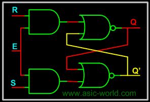
| | We have seen this circuit earlier with two possible input configurations: one with level sensitive input and one with edge sensitive input. The circuit below shows the level sensitive RS latch. Control signal "Enable" E is used to gate the input S and R to the RS Latch. When Enable E is HIGH, both the AND gates act as buffers and thus R and S appears at the RS latch input and it functions like a normal RS latch. When Enable E is LOW, it drives LOW to both inputs of RS latch. As we saw in previous page, when both inputs of a NOR latch are low, values are retained (i.e. the output does not change). |
| | | |
| |  |
| | | |
| | | Setup and Hold Time |
| | For synchronous flip-flops, we have special requirements for the inputs with respect to clock signal input. They are |
| | | |
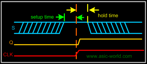
| | - Setup Time: Minimum time period during which data must be stable before the clock makes a valid transition. For example, for a posedge triggered flip-flop, with a setup time of 2 ns, Input Data (i.e. R and S in the case of RS flip-flop) should be stable for at least 2 ns before clock makes transition from 0 to 1.
- Hold Time: Minimum time period during which data must be stable after the clock has made a valid transition. For example, for a posedge triggered flip-flop, with a hold time of 1 ns. Input Data (i.e. R and S in the case of RS flip-flop) should be stable for at least 1 ns after clock has made transition from 0 to 1.
|
| | | |
| | If data makes transition within this setup window and before the hold window, then the flip-flop output is not predictable, and flip-flop enters what is known as meta stable state. In this state flip-flop output oscillates between 0 and 1. It takes some time for the flip-flop to settle down. The whole process is called metastability. You could refer to tidbits section to know more information on this topic. |
| | | |
| | The waveform below shows input S (R is not shown), and CLK and output Q (Q' is not shown) for a SR posedge flip-flop. |
| | | |
| |  |
| | | |
| | |
| | | |
| | | D Latch |
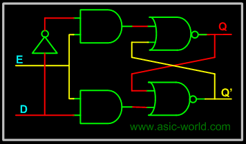
| | The RS latch seen earlier contains ambiguous state; to eliminate this condition we can ensure that S and R are never equal. This is done by connecting S and R together with an inverter. Thus we have D Latch: the same as the RS latch, with the only difference that there is only one input, instead of two (R and S). This input is called D or Data input. D latch is called D transparent latch for the reasons explained earlier. Delay flip-flop or delay latch is another name used. Below is the truth table and circuit of D latch. |
| | | |
| | In real world designs (ASIC/FPGA Designs) only D latches/Flip-Flops are used. |
| | | |
| |  |
| | | |
| | |
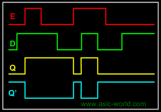
| | Below is the D latch waveform, which is similar to the RS latch one, but with R removed. |
| | | |
| |  |
| | | |
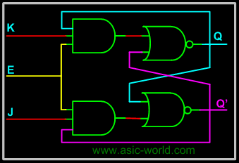
| | | JK Latch |
| | The ambiguous state output in the RS latch was eliminated in the D latch by joining the inputs with an inverter. But the D latch has a single input. JK latch is similar to RS latch in that it has 2 inputs J and K as shown figure below. The ambiguous state has been eliminated here: when both inputs are high, output toggles. The only difference we see here is output feedback to inputs, which is not there in the RS latch. |
| | | |
| |  |
| | | |
| | |
| | | |
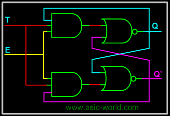
| | | T Latch |
| | When the two inputs of JK latch are shorted, a T Latch is formed. It is called T latch as, when input is held HIGH, output toggles. |
| | | |
| |  |
| | | |
| | |
| | | |

No comments:
Post a Comment