|
| Logic Circuits |
| | | |
| | Boolean algebra is ideal for expressing the behavior of logic circuits. |
| | | |
| | A circuit can be expressed as a logic design and implemented as a collection of individual connected logic gates. |
| | | |
| |  | Fixed Logic Systems |
| | A fixed logic system has two possible choices for representing true and false. |
| | | |
| |  | Positive Logic |
| | In a positive logic system, a high voltage is used to represent logical true (1), and a low voltage for a logical false (0). |
| | | |
| | | Negative Logic |
| | In a negative logic system, a low voltage is used to represent logical true (1), and a high voltage for a logical false (0). |
| | | |
| | In positive logic circuits it is normal to use +5V for true and 0V for false. |
| | | |
| | |
| | | |
| | | Switching Circuits |
| | The abstract logic described previously can be implemented as an actual circuit. Switches are left open for logic 0 and closed for logic 1. |
| | | |
| | | Two variable AND circuit X.Y |
| | | |
| | 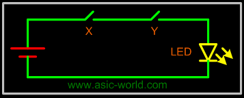 |
| | | |
| | | Two variable OR circuit X + Y |
| | | |
| | 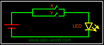 |
| | | |
| | | Four variable circuit U.V.(X + Y) |
| | | |
| | 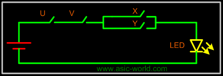 |
| | | |
| | | Truth Table |
| | A truth table is a means for describing how a logic circuit's output depends on the logic levels present at the circuit's inputs. |
| | | |
| | In the following twos-inputs logic circuit, the table lists all possible combinations of logic levels present at inputs X and Y along with the corresponding output level F. |
| | | |
| | 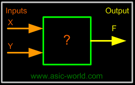 |
| | | |
| |
X | Y | F = X*Y |
0 | 0 | 0 |
0 | 1 | 0 |
1 | 0 | 0 |
1 | 1 | 1 |
|
| | | |
| | When either input X AND Y is 1, the output F is 1. Therefore the "?" in the box is an AND gate. |
| | | |
| | | |
| | | |
| | |

No comments:
Post a Comment